In this tutorial, we will learn about one of the most important concepts in the semiconductor electronics i.e. the PN Junction. Although it is not discussed majorly outside the concept of PN Junction Diode and sometimes the Transistor, a PN Junction is an essential topic in semiconductor electronics.
So, in this PN Junction tutorial, we will discuss some of the basics of a PN Junction, how a PN Junction is formed, characteristics of PN Junction and many other aspects.
Outline
ToggleIntroduction
When talking about semiconductor devices like diodes, transistors and others, PN Junction forms the basis of it. Few semiconductor devices like Photoconductors, for example, are usually formed by doping a single type of impurity. But this is a limited case scenario and most of the semiconductor devices need both types of doping.
A PN Junction is basically formed by introducing (called as Doping) acceptor impurities on one side of a semiconductor crystal while the other side is doped with donor impurities.
The interface between these two regions is called a PN Junction.
Semiconductor Electronics Basics
The electrical conductivity of a semiconductor for instance silicon or germanium depends on the concentration of electrical carriers within the conduction band. The properties of conductivity rely upon the number of dopants present in the doping process.
The conductivity of Silicon is accumulated by a factor 103 at room temperature by the addition of 1 Boron atom per 105 Silicon atoms.
An N-type semiconductor is created by doping the silicon crystal with pentavalent impurity like Antimony and a P-type semiconductor is formed by doping the silicon crystal with trivalent impurity like Boron in tiny concentration.
Both antimony and boron are the essential semiconductor impurities utilized in the process of doping; hence they are referred to as “metalloids”. Individually both the N-type and P-type semiconductors are electrically neutral.
How is a PN Junction Formed?
PN junction is created in a single semiconductor crystal by doping one side of the crystal with acceptor impurity atoms building it as P-type and doping the opposite side with donor impurity atoms building it as N-type. The region where the P-type and N-type converge is referred to as PN junction.
In the region of PN junction, the electrons in the N-type material scatter the junction and combines with the holes in the P-type material. The region of P-type material which is close to the junction in the semiconductor takes on the negative charge for the rationale that the electrons are get attracted by the holes.
As the electrons are departed from the N-type region, it takes on the positive charge. Therefore, at the junction there is an inclination for the free electrons to diffuse into the P-type region and holes to the N-type region and this process is named as diffusion.
The skinny layer sandwiched between these two regions is depleted of majority carriers are referred to as the depletion region. The state of equilibrium of PN junction is defined as the state wherever the PN junction is left without any external electrical potential applied to it.
This can be also be additionally defined as the state of zero voltage bias condition. The width of the depletion region is incredibly thin, typically a few thousands of millimetres, current may not flow through the diode.
PN Junction when Potential is Applied
Different properties are noticed, depending on the width of the depletion region. If the positive potential is applied in such away the P type area becomes positive and therefore the N type becomes negative, holes travel towards the negative voltage.
Equally electrons move towards the positive voltage and jump the depletion layer. The charge density of P-type in the depletion region is staffed with negatively charged acceptor ions as a result the charge density of N-type becomes positive.
Potential barrier constitutes the partition of charge carriers in the middle of the PN junction. This potential barrier should overcome by an external electric potential resource to make the PN junction to conduct electric current.
The formation of the junction and potential barrier in the semiconductor diode happens throughout the manufacturing process of the PN junction semiconductor diode. The degree of the potential barrier may be a function of the materials used in manufacturing of PN junction diodes.
Silicon PN junction semiconductor diode has excellent potential barrier magnitude than germanium PN junction diodes.
PN Junction
A PN junction is fabricated by sticking both the P-type and N-type within the same semiconductor crystal itself. The majority charge carriers in P-type is positively charged holes and in N-type is negatively charged electrons.
The overall charge on both sides of a PN Junction must be equal and opposite to keep up a neutral charge condition around the junction owing to electron-hole pair. The layer between the P-type and N-type where the charge carriers are replicated multiple times is noted as depletion region.
In the equilibrium state no conduction takes place at the PN junction. The conduction of PN junction involves the majority charge carriers diffusion and minority charge carriers drift. Conduction of electrical current in PN junction physically involves in both conduction band and valence band.
Once the external battery is provided the flow of electrons takes place in the conduction band, whereas the flow of holes takes place in the valence band.
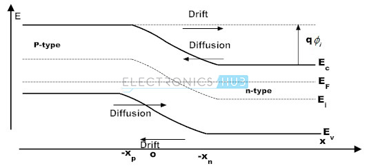
At zero voltage bias equilibrium condition, the minority concentration of holes and electrons will drift simply under the influence of incorporating electric field E. The diffusion of majority charge carriers have to cross the potential barrier VB of the PN junction formed as the effect of the depletion region.
This shall mean that majority charge carriers of the N-type and P-type should at least attain energy of qVB electron volts (eV) before it will surmount the barrier and diffuse into either P-type or N-type region.
The shift of electrons from N side of the PN junction to holes annihilated on the P side of the PN junction produces a potential barrier voltage. The value of barrier voltage is close to 0.6 to 0.7 V in silicon, 0.3 V in germanium and varies with the levels of doping in different semiconductors.
The blocks of P-type and N-type semiconductors in contact with each other have no exploitable properties. Potential barrier must be crossed by the external voltage source to make the PN junction to conduct electricity. If a source of potential is connected in such a way that positive terminal is connected to P side and the negative terminal is connected to the N side.
The negative terminal provides the electrons to the N-type to diffuse towards the depletion layer. Equally the positive terminal removes the electrons in the P-type creating holes that diffuse towards the depletion region.
If the battery supply is big enough to overcome the barrier voltage, then the majority charge carriers from N-type and P-type combine and deplete the junction. As a result more number of charge carriers is replicated and flows towards the depletion region as long as the applied potential is greater than the potential barrier.
Therefore majority charge current is conducted and flows towards the junction. During this approach once the current is conducted owing to majority charge carriers, the PN junction is said to be forward biased.
If the battery terminals are reversed, then the majority charge carriers of N-type are attracted by the positive terminal from the PN junction and the holes are attracted by the negative terminal far from the PN junction.
The width of the depletion layer increases with the applied potential, as a result the recombination of charge carriers at the depletion layer do not takes place. Therefore, no conduction of electric current takes place. During this approach the PN junction is said to be reverse biased.
Built in Potential of PN Junction
The majority charge carriers in the N-type region, i.e., electrons can cross the junction so as to recombine with majority charge carriers in the P-type region i.e. holes. As a result, a negative static space charge builds up in the P-type region as a result of the trivalent impurity boron atoms have a static negative charge as they unleash a positively-charged hole in the valence band.
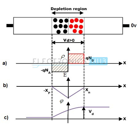
Whereas a positive space charge is formed in the N-type region for the similar reasons. The small volume where this space charge is created is referred to as the space charge zone or depletion zone. As there is a powerful electric field in this small volume, the density of free charge carriers is negligible at thermal equilibrium state.
If the P-type and N-type semiconductors are bringing nearer, a possible potential barrier is developed at the depletion layer. In fact, the static space charges are accumulated at the borders of the PN junction, positive charges in the N-type region and negative charges in the P-type region creates an electrical field ranging from N-type to P-type, that prevents diffusion and added recombination of electrons and holes.
Diffusion is stopped by the formation of the internal electric field. As a result of the existence of this double layer of charges on either side of the PN junction, potential barrier varies sharply within the depletion zone and the potential difference Vd, called the diffusion potential or built-in potential reach non-negligible values.
Electrostatic potential is constant all over the crystal together with the space charge zone, because this potential takes into consideration not only the electric field but also the concentration of charge carriers. The built in potential due to the concentration of charge carriers compensates accurately for the electrostatic potential.
The built-in potential or diffusion potential is proportional to the difference of the Fermi energies of the two unbounded semiconductors:
E = (1/q)*{EFp – EFn} = (kT/q)ln{[NAND]/ni2}
Where
- E is the zero bias junction voltage
- (kT/q) the thermal voltage of 26mV at room temperature.
- NA and NB are the impurity concentrations of acceptor atoms and donor atoms
- n is the intrinsic concentration.
The built-in potential or junction potential of a semiconductor equals the potential across the depletion region in thermal equilibrium state. As the thermal equilibrium implies that the Fermi energy is constant throughout the PN diode device.
The Fermi energies of the conduction band and valence band are therefore shifted up or down, and exhibit a sleek deviation across the region of depletion layer. As a result, there is an electrostatic potential energy difference showing between the P-type and N-type regions, equal to qVd.
The external potential needed to overcome the junction potential relies on the operating temperature and also the kind of semiconductor. Even if the external potential is not applied to the semiconductor, there exists some barrier potential due to electron-hole pair.
PN junction is formed on the single semiconductor and electrical contacts are laid around the semiconductor surface to enable the electrical connection for the external power supply. As a result of it the final device is termed as a PN junction diode or signal diode.


