Outline
ToggleWhat is a Tunnel Diode?
A Tunnel Diode is a heavily doped p-n junction diode. The tunnel diode shows negative resistance. When voltage value increases, current flow decreases. Tunnel diode works based on Tunnel Effect.
The following image shows the symbol of a Tunnel Diode.
Leo Esaki invented Tunnel diode in August 1957. Therefore, it is also called as Esaki diode. The materials used for this diode are Germanium, Gallium arsenide and other silicon materials. Tunnel diode shows a negative resistance in their operating range. So, it can be used as amplifier, oscillators and in any switching circuits.
Width of the Depletion Region in Tunnel Diode
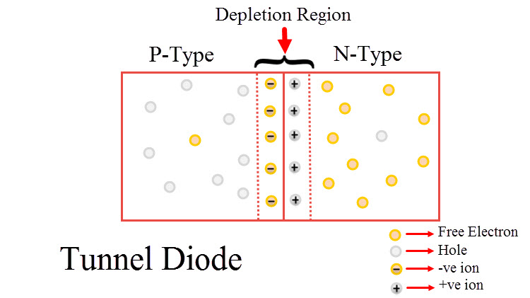
When mobile charge carriers both free electrons and holes are missing, the region in a p-n junction has a region called Depletion region. To stop the flow of electrons from the n-type semiconductor and holes from the p-type semiconductor, depletion region acts as a barrier.
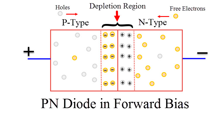
Depending on the number of impurities added, width of depletion region varies. To increase electrical conductivity of the p-type and n-type semiconductor impurities are added. A wide and big depletion region is formed when a smaller number of impurities is added to p-n junction diode. At the same time, when a greater number of impurities is added, narrow depletion region occurs.
The p-type and n-type semiconductor is heavily doped in a tunnel diode due to a greater number of impurities. Heavy doping results in a narrow depletion region. When compared to a normal p-n junction diode, tunnel diode has a narrow depletion width. Therefore, when small amount of voltage is applied, it produces enough electric current in the tunnel diode.
Tunneling Effect
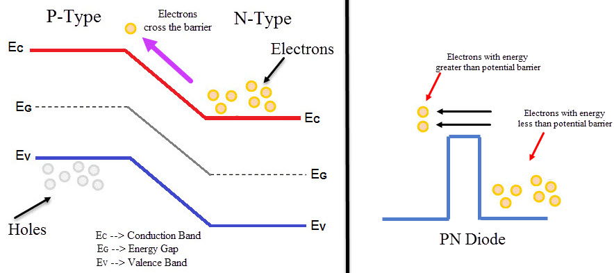
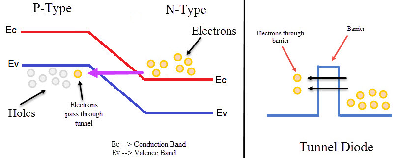
In electronics, Tunneling is known as a direct flow of electrons across the small depletion region from n-side conduction band into the p-side valence band. In a p-n junction diode, both positive and negative ions form the depletion region. Due to these ions, in-built electric potential or electric field is present in the depletion region. This electric field gives an electric force to the opposite direction of externally applied voltage.
As the width of the depletion layer reduces, charge carriers can easily cross the junction. Charge carriers do not need any form of kinetic energy to move across the junction. Instead, carriers punch through junction. This effect is called Tunneling and hence the diode is called Tunnel Diode.
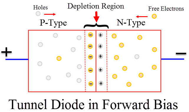
Due to Tunneling, when the value of forward voltage is low value of forward current generated will be high. It can operate in forward biased as well as in reverse biased. Due to high doping, it can operate in reverse biased. Due to the reduction in barrier potential, the value of reverse breakdown voltage also reduces. It reaches a value of zero. Due to this small reverse voltage leads to diode breakdown. Hence, this creates negative resistance region.
Tunnel Diode Working Phenomenon
Unbiased Tunnel Diode
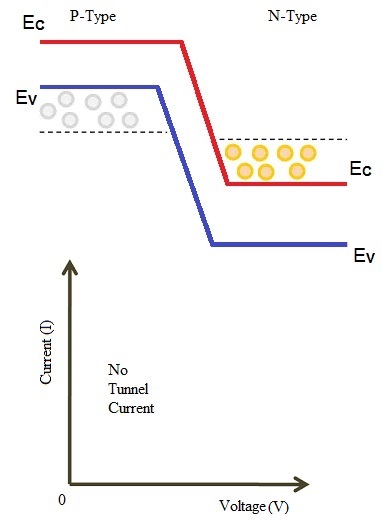
In an unbiased tunnel diode, no voltage will be applied to the tunnel diode. Here, due to heavy doping conduction band of n – type semiconductor overlaps with valence band of p – type material. Electrons from n side and holes from p side overlap with each other and they will be at same energy level.
Some electrons tunnel from the conduction band of n-region to the valence band of p-region when temperature increases. Similarly, holes will move from valence band of p-region to the conduction band of n-region. Finally, the net current will be zero since equal numbers of electrons are holes flow in opposite direction.
P α e (-A *E *b *W)
P – Probability that the particle crosses the barrier
W – Width of the barrier
E – Energy of the barrier
Small Voltage Applied to the Tunnel Diode
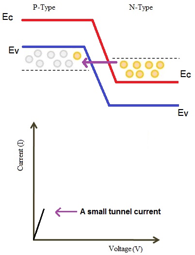
When a small voltage, that has lesser value than the built-in voltage of the depletion layer, is applied to the tunnel diode, there is no flow of forward current through the junction. Nevertheless, a minimal number of electrons from the conduction band of n region will start tunneling to valence band in p region.
Therefore, this movement creates a small forward biased tunnel current. When a small voltage is applied, tunnel current starts to flow.
Increased Voltage Applied to the Tunnel Diode
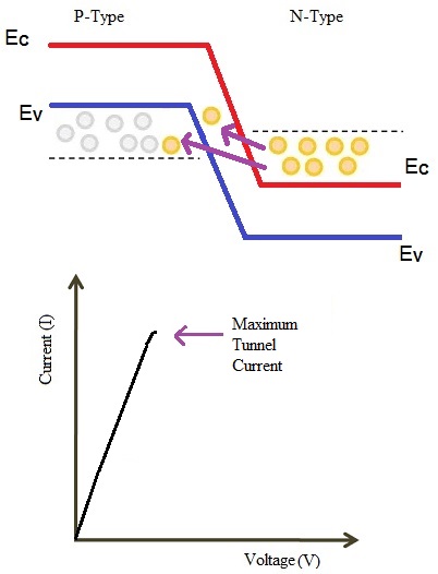
When the amount of voltage applied is increased, the number of free electrons generated at n side and holes at p side is also increased. Due to voltage increase, overlapping between the bands are also increased.
Maximum tunnel current flows when the energy level of n-side conduction band and the energy level of a p-side valence band becomes equal.
Further Increased Voltage Applied to the Tunnel Diode
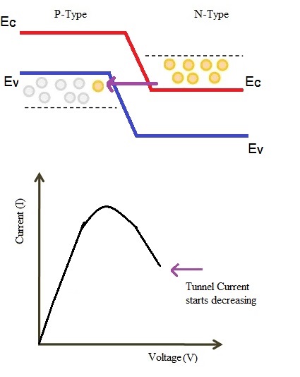
A further increase in the applied voltage will cause a slight misalignment of the conduction band and valence band. Still there will be an overlap between conduction band and valence band. The electrons move from conduction band to valence band of p region. Therefore, this causes small current to flow. Hence, tunnel current starts decreasing.
Largely Increased Voltage Applied to the Tunnel Diode
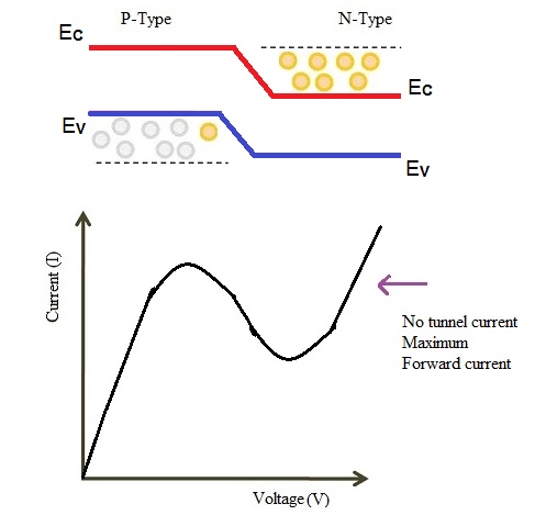
The tunneling current will be zero when applied voltage is increased more to the maximum. At this voltage levels, the valence band and the conduction band does not overlap. This makes tunnel diode to operate same as a PN junction diode.
When applied voltage is more than the built-in potential of the depletion layer the forward current starts flowing through the tunnel diode. In this condition, current portion in the curve decreases when the voltage increases and this is the negative resistance of tunnel diode. Such diodes operating in negative resistance region is used as amplifier or oscillator.
V-I Characteristics of Tunnel Diode
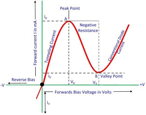
Due to forward biasing, because of heavy doping conduction happens in the diode. The maximum current that a diode reaches is Ip and voltage applied is Vp. The current value decreases, when more amount of voltage is applied. Current keeps decreasing until it reaches a minimal value.
The small minimal value of current is Iv. From the above graph, it is seen that from point A to B current reduces when voltage increases. That is the negative resistance region of diode. In this region, tunnel diode produces power instead of absorbing it.
Applications of Tunnel Diode
- Tunnel diode can be used as a switch, amplifier, and oscillator.
- Since it shows a fast response, it is used as high frequency component.
- Tunnel diode acts as logic memory storage device.
- They are used in oscillator circuits, and in FM receivers. Since it is a low current device, it is not used more.



2 Responses
Great post ! thanks for telling about tunnel diode in detail. thanks for giving the detailed correct information. Sir i always follow your blogs.
It was too informative, thanks!