Introduction
A Diode is an electronic component that has two terminals and allows current to flow only in one direction. Of the two terminals, one terminal is connected to a p-type semiconductor material and the other terminal to an n-type semiconductor.
Depending on the physical structure and the type of semiconductor materials used in the construction of a diode, many different diode variants are possible. They range from diodes with optical properties like photo-diodes, LEDs, laser diodes etc., to the ones like rectifier, Zener and Tunnel diodes.
In this article we will look at one such variant of the diode – the Varactor Diode.
For comprehensive details of different types of diodes, visit this page: Different Types of Diodes
What is a Varactor Diode?
A Varactor Diode (also known with the names Varicap Diode, Varactor Diode, Tuning Diode) is a p-n junction diode which acts as a variable capacitor under varying reverse bias voltage across its terminals.
In other words, it is a specially designed semiconductor diode whose capacitance at the p-n semiconductor junction changes with the change in voltage applied across its terminals. And because it is a diode that can behave as a variable capacitor, it is named as a Varactor Diode in short.
It is mainly used to replace variable capacitors that need to be operated mechanically for changing the value of capacitance. One advantage is that the capacitance of a varactor diode can be changed just by changing the voltage across its terminals. We will learn more about its operation in the following sections.
Symbolic Representation
A number of schematic symbols are used to represent a Varactor Diode in circuit diagrams. Of them, the three most popular representations are shown below:
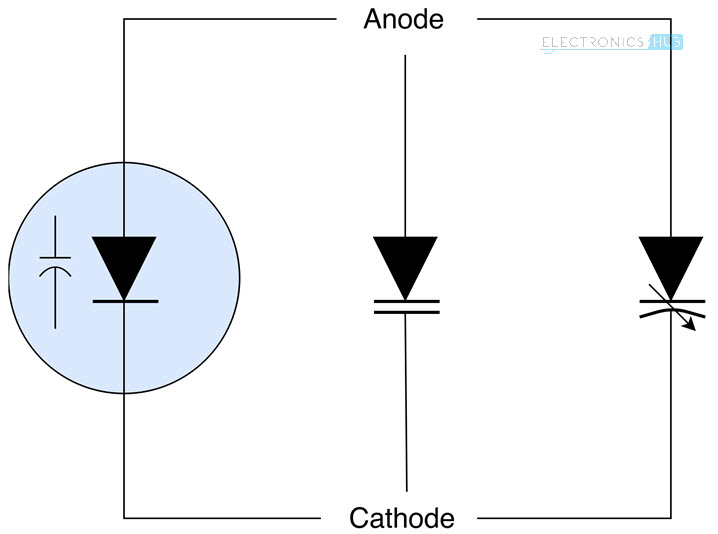 Among these three symbols of a Varactor Diode, the second symbol is more frequently used. It is a combination of symbol of a p-n junction diode and a capacitor. In the symbol, the triangle indicates the presence of a diode component, and the two lines at the tip of triangle indicate parallel plates of a capacitor.
Construction
A Varactor Diode consists of p-type and n-type semiconductor layers sandwiched together, with the n-type layer attached to a mesa (table-shaped) structure. A gold plated molybdenum stud is connected to n-type layer via the mesa structure and it acts as cathode terminal.
The p-type layer is connected to another gold plated molybdenum stud (which acts as anode) via a gold wire. Except for some portion of the molybdenum studs, the entire arrangement is enclosed in a ceramic layer.
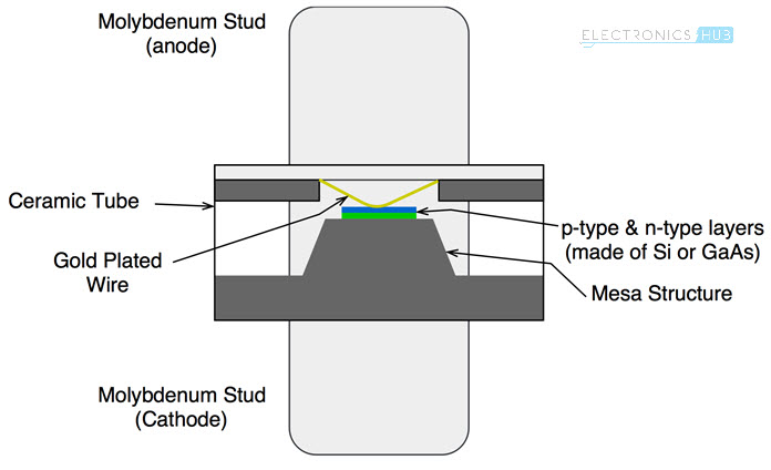
The p-type and n-type layers of the varactor diode are made up of silicon or gallium arsenide depending on the type of application for which it is used. For low frequency applications, silicon is used, and for high-frequency applications gallium arsenide is used.
For conventional diodes, the p-type and n-type semiconductor layers are uniformly doped with impurities to improve conductivity. But in the case of varactor diodes, the concentration of impurities near the pn junction is very less and it gradually increases as we move towards the layer’s other surface.
Working
To learn how a varactor diode works, you need to first understand the working principle of a variable capacitor:
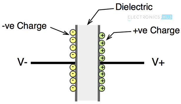
A capacitor consists of two conducting surfaces separated by a non-conducting dielectric medium (see figure below). When one of surfaces is connected to a positive voltage and the other to negative voltage, because of attraction between positive and negative carriers, positive charge accumulates on one surface and negative charge on the other.
The amount of charge that accumulates is termed as capacitance. If we reduce the gap between the two surfaces, the force of attraction between positive and negative charge carriers increases and so more charge accumulates on the surface i.e. the capacitance increases.
The opposite happens when the surfaces are moved away from each other i.e. the capacitance decreases. A variable capacitor has a mechanical arrangement which allows us to change the gap between surfaces, which effectively changes the capacitance.
 Let us now come back to working of a p-n junction diode. The p-type layer of the diode is filled with positive charge carriers and the n-type layer with negative charge carriers. Near the surface of contact between the two layers, positive and negative charges diffuse and neutralize each other. This region is known as depletion region.
No further diffusion of charge carriers through the depletion layer is possible unless an external voltage is applied. So effectively the depletion layer acts as an insulator.
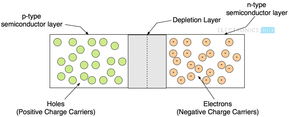
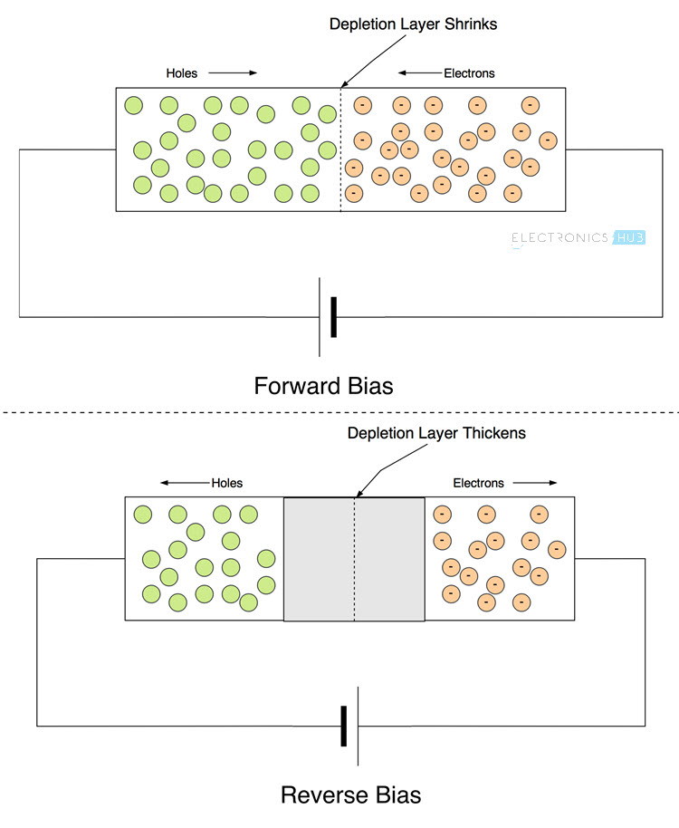
The width of depletion layer depends on the voltage applied across the p and n-type layers. If a forward bias voltage is applied, i.e. positive voltage is applied to the p-type layer and negative voltage is applied to the n-type layer, the width of depletion decreases, and above a certain voltage it completely disappears.
If a reverse bias is applied, i.e., positive voltage to n-type layer and negative voltage to p-type layer, the width of depletion layer increases. The below diagram illustrates the two scenarios:
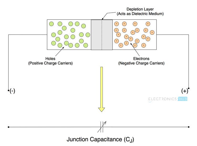
Simply put, the width of the depletion region can be changed to a required value just by adjusting the voltage across the p & n-type semiconductor layers. So, by now you must have observed the similarities between capacitor, and the diode in reverse bias. The depletion layer in the diode is akin to the dielectric medium in a capacitor, which acts as an insulator and prevents the flow of charge carriers from one side to the other.
So, when reverse bias voltage is applied across the diode, respective charge carriers accumulate on either side of the depletion layer. This makes the diode acquire some capacitance and it is termed as junction capacitance.
A Varactor Diode is specially designed to enhance this ability to store charge carriers when reverse bias is applied, thus allowing it to act as a capacitor.
The junction capacitance is inversely proportional to the width of depletion layer i.e. if the width of depletion layer is less, the capacitance will be more, and vice versa. So if we need to increase the capacitance of a varactor diode, the reverse bias voltage should be decreased. It causes the width of depletion layer to decrease, resulting in higher capacitance. Similarly increasing the reverse bias voltage should decrease the capacitance.
This ability to get different values of capacitances just by changing the voltage applied is the biggest advantage of a varactor diode when compared with a normal variable capacitor.
Characteristics
The below graph illustrates the relation between the magnitude of reverse bias voltage p-type & n-type layers of a varactor diode, and the magnitude of junction capacitance.
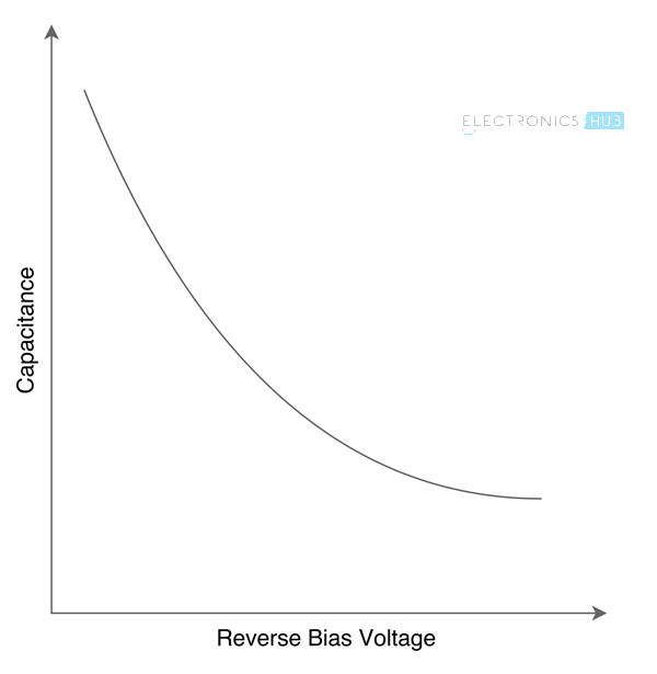
You can observe that the junction capacitance of a varactor diode is inversely proportional to reverse bias voltage. Also because of difference in the way impurities are added to the p-type and n-type layers, the capacitance of a varactor diode is always higher than that of a conventional diode.
The exact magnitude of junction capacitance of a varactor diode is calculated with respect to the capacitance at zero-bias condition (CJ), forward bias voltage (Voltage required to remove depletion layer completely, VB) and the actual reverse bias voltage (VR) applied across the junction. It is given by the formula:
CJ = C0(1 + VR/VB)-n
‘n’ is a constant and varies depending on the way p and n-type layers are doped. Its value lies between (0.5 – 0.33). The value of reverse bias voltage (VR) should be below the breakdown voltage, above which the value of capacitance CJ equals zero because of breakdown of depletion region and the free flow of holes and electrons.
Equivalent Circuit
For designing circuits that use the properties of a varactor diode, we first need to break down its electrical properties and visualize an equivalent circuit with basic components like resistors, capacitors and inductors. The below image shows such approximate equivalent circuit of a varactor diode when operated under reverse bias condition.
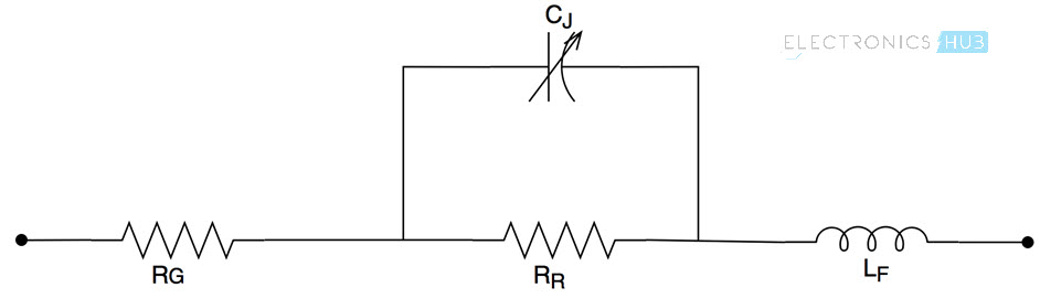
RR is the reverse bias resistance and RG is the geometric resistance of the varactor diode. CJ is the junction capacitance which is dependent on the reverse bias voltage. LF is the effective inductance and it depends on the frequency limits under which a varactor diode should be operated.
Applications
Owing to the special property of varying capacitance with varying voltage, varactor diodes are mostly used in frequency modulation or tuning circuits where the value of capacitance determines the output modulation frequency. Some of the other applications include:
- Automatic Frequency Controllers (AFCs)
- Ultra High Frequency Television sets
- High frequency Radios
- Frequency Multipliers
- Band Pass Filters
- Harmonic Generators

5 Responses
It was very useful information for me
Thanks a lot
Nice explanation….
Useful information
It was very useful for me personally