What is Schottky Diode?
Schottky diode is a device, which comes under the type of a metal – semiconductor junction diode. Barrier diode and low voltage diodes are the other names for Schottky diode. When compared to a PN junction diode, power drop is lower in Schottky diode. A scientist named Walter.H.Schottky first discovered Schottky diode.
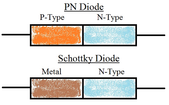
Generally, in a PN junction device, when positive type (p-type) and negative type (n-type) are joined together they form a PN junction. However, in a Schottky diode, materials like aluminum or platinum are used instead of P type semiconductors.
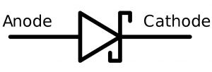
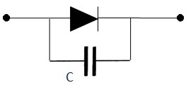
Symbol of Schottky Diode
The following image shows the symbol of a Schottky Diode.
Working of Schottky Diode
The most important physical parameter of this Schottky diode is their fast switching rate and less forward voltage drop. It is a metal – semiconductor junction that does not have the capacity to store charges at their junction. The reason behind this is due to absence of depletion layer.
Usually, a voltage drop happens across the diode terminals, when current flows through a diode. Schottky diode voltage drop is usually between 0.15 and 0.45 volts when compared to a normal diode. A normal PN junction diode has a voltage drop ranging between 0.6 to 1.7 volts. For a better efficiency and output, voltage drop should be low. When manufacturing the diode, N-type semiconductor acts as a cathode and the metal side acts an anode of the diode.
When voltage is given to the diode, the current flows in the forward direction. When this current flows through the diode, there will be a minimum voltage loss across the terminals of the diode. This loss of voltage is called as Voltage drop.
Construction of Schottky Diode
It is made of a metal and semiconductor forming unilateral junction. Few metals like gold, silver, molybdenum, tungsten or platinum are utilized. Usually an N type semiconductor, which includes Gallium, is used. Silicon is used for low frequency operation.
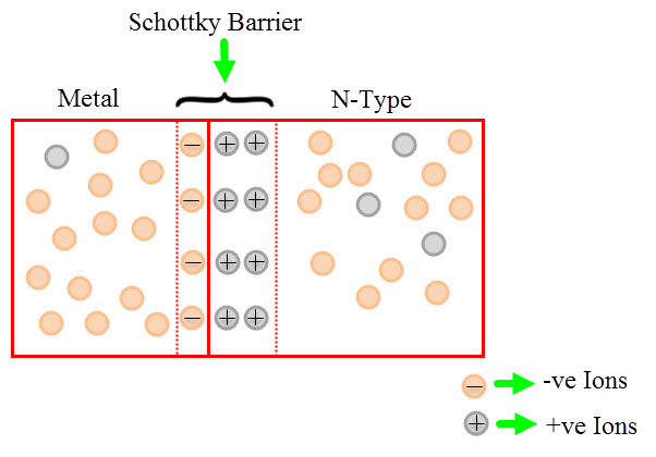
Schottky diode is related directly with temperature dropping. In N type semiconductor, decrease and increase of temperature doping concentration happens. Between the semiconductors–metal junctions, a depletion layer is formed known as Schottky barrier.
This barrier is called as potential energy barrier. Two types of Schottky barriers are Rectifying and Non-rectifying type. When a metal and lightly doped semiconductor meets each other, the Schottky barrier is formed. Sequentially when a metal encounters the heavily doped semiconductor, it forms a non-rectifying barrier. The width of depletion layer rises when the semiconductor doping increases. At the same time, when width decreases charge carriers travels through tunnel and reaches the depletion layer. When doping level increases, the junction does not act as rectifier and it becomes ohmic contact.
Under unbiased condition, electrons accumulated on the semiconductor side will have a lower energy level than electrons present on the metal region. Due to this reason, electrons cannot flow across the Schottky Barrier. Under forward biased condition, an electron present in the N-side receives more energy to cross the junction barrier and enters into the metal. Due to this, the electrons are also called as hot carrier. Hence, diode is called as hot carrier Diode.
The Schottky diode can be represented as an electrical equivalent circuit with typical values of the components is shown below.
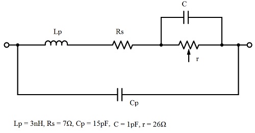
The above circuit is minimized as shown below. This approximated circuit is used in many applications.
Specialties of Schottky Diode
- Due to the absence of the current flow from metal to N-type semiconductor, it acts as a unipolar device. Whereas, a PN junction diode is a bipolar device.
- The metal does not have any holes, it does not store any charge. Due to this reason, Schottky diode has the advantage to quickly switch with relatively low noise.
- It has a low barrier potential compared to PN diode.
Operation of Schottky Diode
Unbiased Schottky Diode
The free electrons present inside the n – type semiconductor will move from n – type semiconductor to a metal during the combination between metal and n – type semiconductor. This results in production of equilibrium state. When free electrons moves across the junction, it provides an extra electron to the atoms present in the atom.
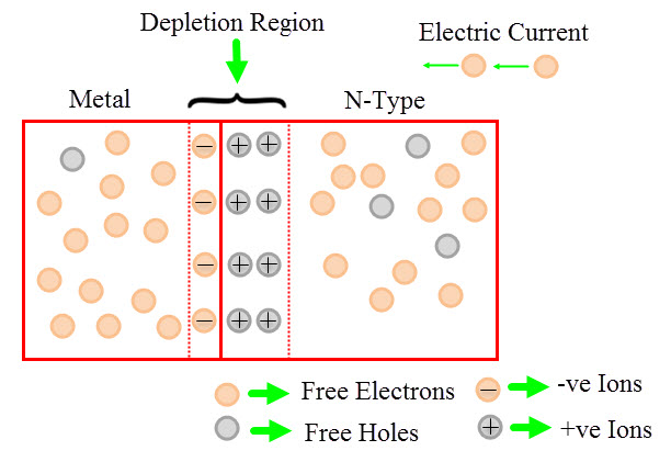
Due to this, atoms present in the metal junction receive an extra electron. The atoms at the negative side junction lose electrons and become positive ions. On the metal junction, atoms will gain extra electrons and tries to become negative ions.
Hence, this will result in production of positive ions at negative side and negative ions on the positive side at the metal junction. Depletion region will be formed when these positive and negative ions comes together. In unbiased Schottky diode, only less number of electrons will flow from semiconductor to metal. Other electron flow is stopped due to the built in voltage.
Forward Biased Schottky Diode
In the n-type semiconductor when positive terminal of the battery is connected to metal and negative terminal is connected to n-type conductor, it is called as Forward biased Schottky diode. On the diode, when forward bias voltage is applied, more electrons are formed in the metal and conductor.
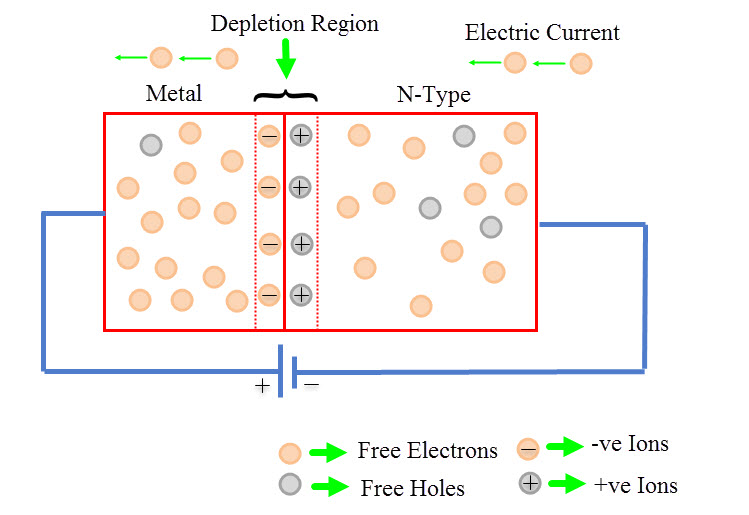
When a voltage greater than 0.2 volts are applied, free electrons cannot move through the junction barrier. Due to this current will flow through diode. When voltage value increases, depletion region becomes thin and disappears.
Reverse Biased Schottky Diode
In the n-type semiconductor if the negative terminal of the battery is coupled to metal and positive terminal is connected to n-type conductor, it is called as Reverse biased Schottky diode. At the same time, if a reverse bias voltage is applied, the width of depletion region increases.
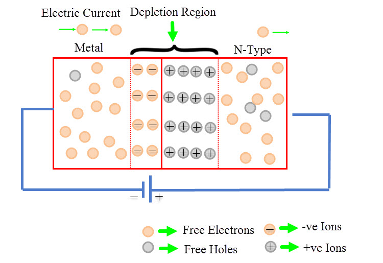
Therefore, the current flow stops. In the metal plate, there will be more number of excited electrons. Due to this, there will be flow of a small amount of leakage current. When reverse biased voltage increases further, current also increases due to weak barrier. When abnormal increase in bias voltage takes place, electric current also increases suddenly. A device will be damaged, when the depletion region breaks down.
V-I Characteristics of Schottky Barrier Diode
The V-I (Voltage-Current) characteristics of Schottky diode is shown in the below figure. Along the graph, the vertical line signifies the current flow and the horizontal line denotes the voltage applied across the Schottky diode. The V-I characteristics of Schottky diode is almost similar to the P-N junction diode.
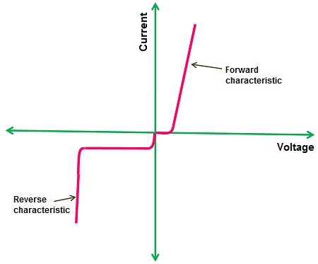
Nevertheless, the forward voltage drop of Schottky diode is very low when compared to the P-N junction diode. The forward voltage drop ranges from 0.3 volts to 0.5 volts. The barrier of forward voltage drop is made of silicon. The forward voltage drop is proportional to the doping concentration of N type semiconductor. Due to high concentration of current carriers, the V-I characteristic of Schottky diode is steeper.
Applications of Schottky Diode
Schottky diodes are used in electronics industry for many applications in diode rectifier because of its properties. They are used for voltage clamping applications, to prevent transistor saturation. It is used as Schottky TTL in digital devices as these devices require fast switching. as the performance of digital computers is determined by switching speed of diodes, Schottky diode is an important component for digital computers.

3 Responses
Schottky Diode is very importent in use of SMPS power supply designs Many people don’t know exactly the difference between ordinary PN junction diodes and SCHOTTY DIODES. This article is valuable to every one those who are in field of ‘ELECTRONICS”
Thanks a lot for your attempt.
DAS LOPEZ
Thank you very much electronicshub team.
Very useful for every student…..
Amazing I in love with your content. And your articles are always helpful.