In this tutorial, we will learn about some of the important Diode Characteristics. By examining these Diode Characteristics, you will have a better understanding of the working of a Diode in general.
Commonly used Diode Characteristics
Some of the frequently used diode characteristics are given below.
- Current Equation
- DC Resistance
- AC Resistance
- Transition Capacitance
- Diffusion Capacitance
- Storage Time
- Transition Time
- Recovery Time
Now, we will see a little bit more about these diode characteristics in brief.
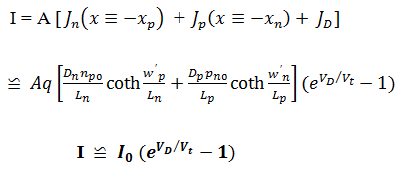
Diode Current Equation
PN junction diode is widely known for passing the electric current solely in one direction. The amount of current flowing through the PN junction diode greatly depends on the type of material used and also depends on the concentration of doping in the fabrication of PN diode.
[adsense1]
The main reason for the flow of current is due to the generation or recombination of majority charge carriers in the structure of the PN junction diode.
We will have three regions responsible for the flow of majority charge carrier current. These regions are namely quasi neutral P – region, depletion region, quasi neutral N – region. The region of the quasi neutral P – type is the separation between the edge of the depletion region and the edge of the diode on the P – side.
The region of the quasi neutral N – type is the separation between the edge of the depletion region and the edge of the diode on the N – side. For assumption, this separation distance is infinity. There will be no variation in the concentration of charge carriers as we move towards the boundaries of the diode. The electric field will not present in the quasi neutral region.
Δnp(x → -∞) = 0
Δpn(x → +∞) = 0
The diode current in the forward bias is due to the recombination of majority charge carriers. The charge carrier recombination takes place either in the P – type or N – type quasi neutral regions, in the depletion region or at the ohmic contacts i.e., at the contact of metal and semiconductor.
The current flow in the reverse bias is due to generation of charge carriers. This type of charge carrier generation process further increases the current flow in forward and also in reverse bias condition.
The flow of current in the PN junction diode is determined by the charge carrier density, the electric field throughout the structure of PN junction diode and the quasi Fermi level energies of the P – type and N – type. The carrier density and the electric field are used for determining the drift current and diffusion current of the PN diode.
[adsense2]
The quasi Fermi level energies of the electrons and holes within the depletion region and that of in the N – type and P – type quasi neutral regions are assumed to be approximately equal in obtaining an analytical solution.
If the Fermi energy levels are assumed to be constant in the depletion region, the minority charge carrier density at the boundary of the depletion region would be as follows,
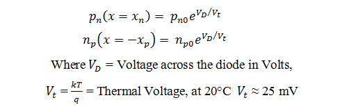
When there is no external voltage applied, thermal equilibrium state is reached at the above stated equations. The separation between the Fermi levels increases with the external applied voltage. This external voltage is multiplied by the charge of the electron.
The excess charge carriers present in either of the quasi region recombines straight away when they reach the metal – semiconductor contact. The process of recombination takes place rapidly at the ohmic contact and it further increases by the presence of metal. Therefore valid boundary conditions can be stated as follows,
pn (x = wn) = pn0
np (x = -wp) = np0
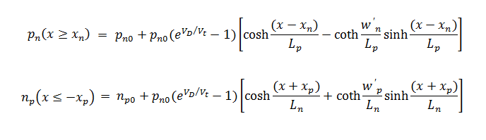
Consider the diffusion current equation for both the quasi neutral regions of N – type and P – type, the expression for the current of the ideal diode will be obtained by the using the boundary conditions to the considered diffusion current equation.
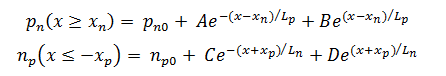
Converting the above equations in terms of hyperbolic functions, rewriting the above equations as
pn (x≥xn) = pn0 + A cosh {(x-xn)/Lp} + B sinh {(x-xn)/Lp}
np (x ≤ -xp) = np0 + C cosh {(x+xp)/Ln} + D sinh {(x+xp)/Ln}
Here A, B, C and D are the constant values to be determined. If the boundary conditions are applied to the above hyperbolic equations, then we will have
Where the widths of the quasi neutral region of N – type and P – type are given as
w´n = wn – xn
w´p = wp – xp
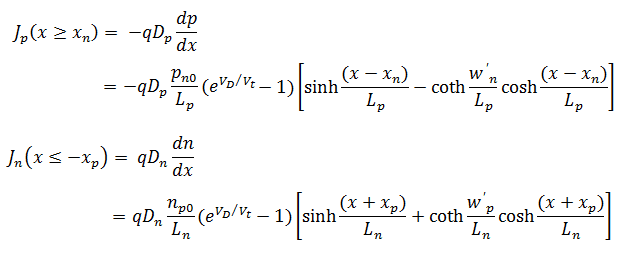
The charge carrier current density in each of the quasi neutral region is calculated from the diffusion current equation as
The amount of electric current flowing throughout the entire structure of the PN junction diode always should be constant, because no charge can disappear or accumulate in entire structure of diode.
Hence, total current through the diode is equal to the sum of the maximum hole current in the n-region, the maximum electron current in the p-region and the current because of the recombination of charge carriers in depletion region. The maximum currents in the quasi neutral regions occur at the sides of the depletion region.
DC or Static Resistance
Static resistance or DC resistance of a PN junction diode defines the diode’s resistive nature when a DC source is connected to it. If an external DC voltage is given to the circuit in which the semiconductor diode is a part of it, results in a Q-point or operating point on the PN junction diode characteristic curve that does not alter with time.
The static resistance at the knee of the curve and below of it will be much greater than the resistance values of the vertical rise section of the characteristic curve. Minimum is the current passing through a diode maximum is the level of DC resistance.
RDC = VDC / IDC
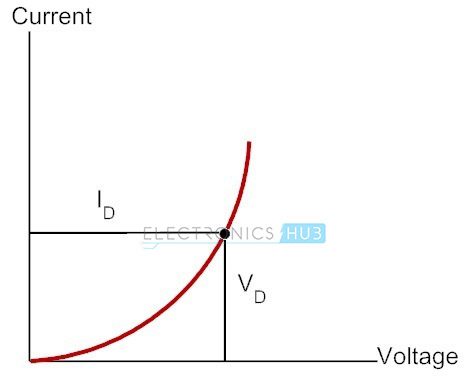
AC or Dynamic Resistance
Dynamic resistance is derived from Shockley’s Diode Equation. It defines the diode resistive nature when an AC source which depends on the DC polarisation of the PN junction diode is connected to it.
If an external sinusoidal signal is given to the circuit consisting of a diode, the altering input will shift the instantaneous Q – point slightly from the current position in the characteristics and therefore it defines a definite change in voltage and current.
When no external alternating signal is applied, the operating point will be the Q – point (or quiescent point) which is determined by the applied DC signal levels. The AC resistance of the diode is increased by lowering the Q-point of operation. In short, it is equivalent to slope of voltage – current of the PN diode.
rd = ΔVd / ΔId
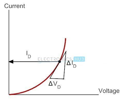
Average AC Resistance
If the input signal is sufficient enough to produce a large swing, then the resistance related to the diode for this region is called as AC average resistance. It is determined by the straight line that is drawn linking the intersection of the minimum and maximum values of external input voltage.
Ravg = ( ΔVd / ΔId ) pt to pt
Transition Capacitance
Transition capacitance can also be termed as depletion layer capacitance or space charge capacitance. It is mainly observed in a reverse biased configuration where the P – type and N – type regions have lower resistances and the depletion layer may act like a dielectric medium.
This type of capacitance is due to the variations in the external voltage where the immobile charges get vary at the edges of the layer of the depletion region. It depends upon the dielectric constant and the width of the depletion layer. If the depletion layer width increases the transition capacitance decreases.
CT = εs / w = √{[qεs / 2(ϕi – VD)][NaNd / (Na + Nd)]}
Diffusion Capacitance
Diffusion capacitance can also be termed as storage capacitance mainly observed in forward biased configuration. It is the capacitance caused by the transport of charge carriers between the two terminals of a diode i.e., from anode to cathode in the forward biased configuration of a PN junction diode.
If the electric current is allowed to pass through the semiconductor device, there will be some charge created across the device at some point of time. In case if the applied external voltage and current changes to a different value, there will be a different amount of charge created in the transit.
The ratio of transiting charge created to the differential change in voltage will be the diffusion capacitance. If the level of current is increased then the diffusion capacitance levels automatically increases.
The increased levels in current will result in reduced levels of associated resistance and also the time constant, that is important in very high-speed applications. The diffusion capacitance value is much greater than the value of transition capacitance and it is directly proportional to the value of direct current.
Cdiff = dQ/dV = [dI(V)/dV]ΓF
Storage Time
The PN junction diode acts like a perfect conductor in forward biased configuration and acts like a perfect insulator in reverse biased configuration. During the switching time from forward to reverse biased condition the current flow switches and remains constant at the same level. This time duration over which the current reverses and maintains constant level is called as storage time (Ts).
The time taken by the electrons to move from P – type back to N- type and holes to move from N – type back to P – type is the storage time. This value can be determined by the geometry of the PN junction. During this storage time the diode behaves as a short circuit.
Transition Time
The time for the current to decrease to a reverse leakage current value after it remains at a constant level is called as a transition time. It is denoted as the transition time value is determined by the geometry of the PN junction and concentration of doping levels of the P – type and N – type materials.
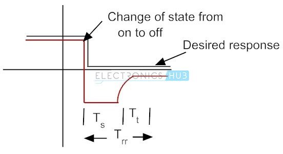
Reverse Recovery Time
The sum of the storage time and transition time is termed as reverse recovery time. It is the time taken by the diode to raise the applied current signal to 10% of the constant state value from the reverse leakage current. The reverse recovery time value for PN junction diode is usually of the order of microseconds.
Its value for a widely used small signal diode rectifier 1N4148 is usually 4 ns and for general purpose rectifier diode it is 2 μs. The fast switching speeds can be achieved by the high value of reverse leakage currents and high forward voltage drops. It is denoted by Trr.
Datasheet Analysis
Summary
A brief view on different Diode Characteristics is presented here.

One Response
Please post more examples and function of each components