Christmas is known as the carnival of lights and every person decorates its house with multicolored lights which we normally purchase from the bazaar. Did you ever have a thought of building your own Christmas lights, which is used to decorate own house or your own house holy place. This very easy circuit will assist you to develop your own decorative lights.
The plus point of these circuits is that you did not require to take tension regarding the ON and OFF of the light. In the evening time, lights automatically become ON while in the morning, it becomes OFF. So it will save your electricity bill when you go away from your house.
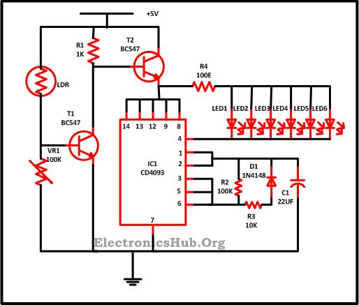
Christmas Lights using LEDs Circuit Diagram:
LED Christmas Lights Circuit Components:
- IC
- CD4093 – 1
- Resistor
- R1 (1K) – 1
- R2 (10K) – 1
- R3 (100K) – 1
- R4 (100E) – 1
- VR1 (100K) – 1
- C1 (22uf) – 1
- T1 (BC547) – 1
- LDR – 1
- D1 (1N4148) – 1
- LED – 6
Component Description:
- LDR – The sensitivity of the LDR based on the intensity of light declining on it. With the increase in the fall of light intensity LDR resistance decreases and vice versa.
- LED – It consists of semiconductor material and produces different colors of light as its output.
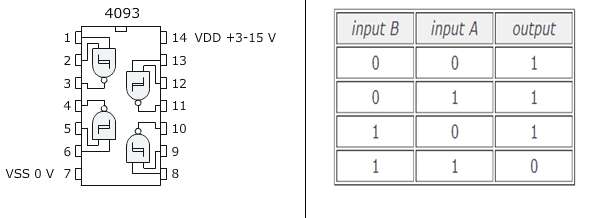
- IC CD4093- It is made up of four Schmitt-trigger circuit. Every circuit work as a NAND gate off two inputs having Schmitt trigger action on both inputs. For positive and negative going signals the gate switches at different points.
LED Christmas Lights Circuit Description:
This circuit is mainly made up of CD4093 IC. It is actually a Schmitt trigger quad NAND gate having two input terminals. All LEDs are employed in this circuit with a sensor along with some other components like transistor, diode and resistors.
IC CD4093 is a Dual lnline Package having 14 pins. Pin 1 can identify with a very tiny notch on the one face of the IC. It is made up of 4 self–sufficient NAND gate on a particular chip. Every gate has its own 2 input terminals and one output terminal. 5V to 15V is the voltage working range of these IC.
It comes in a 14 pin Dual Inline Package (DIP). It will carry on an average of 10 MA of current at a voltage of 12V but it can trim down by reducing the power supply voltage.
Out of 14 pin package pin number 14 and 7 is used for connecting battery or power supply. Pin 7 is attached with the negative terminal while pin 14 is attached to the power supply. As we have already familiar that it is consist of four gates we named them as NI1, NI2, NI3 and NI4.In the first gate i.e. NI1 pin 1 and 2 is for the input purpose while pin 3 is for the output. You can find in the circuit diagram shown below. When all the input terminal is in high state the output moves toward the low state, or else we will obtain high output. This can be employed in the truth table drawn below.
This whole circuit is parted into two parts first one is for the sensor section and the second one is for the LED flesher section. The light sensing part of the circuit is constructed using LDR along with two transistors namely T1 and T2. During the day time light resistance of LDR is low which in turn make the transistor T1 into transmission due to this T2 transistor voltage goes to the low state and left over in the cut off state. That is why during the day time LED attached at the output point will not shine. While at the time of night when no light is present LDR, LDR reaches to high resistance, as a result of it conduction of T1 stops and T2 begins its conduction. Due to its LED attached at the output starts glowing.
At this instant, LED flashing circuit is constructed around CD4093 IC which is functioning in oscillator mode. With the assistance of resistor R2 and capacitor C1 oscillation part is being created. The fleshing effect is being generated with the Diode D1 along with the resistor R3 as it causes speedy alteration of the capacitor C1. So when the charging of the capacitor C1 reaches to the half of the power supply , output from the pin3 IC1 move lower and the capacitor C1 discharges. From the circuit diagram shown you can find that pin3 is linked withpin5 as well as pin 6 hence the capacitor C1 again charges. So the above cycle keeps on going till the time power is supplied in the circuit.
By altering the value of the resistor R2 as well as capacitor C1, you can enlarge or reduce the rate of the LED flashing. Suppose you want to enlarge the flashing light then just reduce the value of C2 capacitor and for reducing the rate just decrease the value of the capacitor. And for maintaining the sensitivity of the LDR in the circuit all you need to use a variable resistor.

9 Responses
idea is good
What a beautiful idea about christmas lights then give an idea of newyear lights.,,,,,
What a beautiful idea about christmas lights then give an idea of newyear lights
I constructed this ciruit..the leds should go on and off in the dark..shouldn’t they..?but they kept shining..could any one help me..
CD4093 IC is this same as flip flop also or not? or is it a kind of sequential circuit?
Hi joan Firstly flip flop is a sequential circuit.Here CD4093 is a Nand Schmitt trigger.
where is pin 10&11. and what is it function
These two pins are left unconnected.
I simulated this circuit on the computer but it didn’t work. Any modifications to be done?