Inverting operational amplifiers are crucial for electronic enthusiasts seeking to invert signal phases with precision control over gain. These amplifiers utilize negative feedback to produce an output 180 degrees out of phase with the input, enabling applications from sensor signal amplification to current-to-voltage conversion.
Understanding their working principles, including virtual ground and voltage gain calculations, provides a solid foundation for designing and optimizing electronic circuits for a variety of applications.
Outline
ToggleHow Does Inverting Op-amplifier Work?
Operational amplifiers can be configured to work as a variety of functional circuits such as amplifiers, oscillators, voltage regulators, filters, rectifiers etc. Most of these circuit configurations require the op-amp output to be connected back to its input.
This connection from output to input is called “feedback”. Since op-amps have two input terminals, positive and negative, the feedback connection in an op-amp can be either positive feedback or negative feedback. If the output is connected to the non-inverting terminal of the op-amp, the feedback is said to be positive and if the output is connected to the inverting input, the feedback is said to be negative. The output is fed back to the input of the op-amp through an external resistor, called feedback resistor (Rf). Feedback connection provides a means to accurately control the gain of the op-amp, depending on the application.
The inverting amplifier is an important circuit configuration using op-amps and it uses a negative feedback connection. An inverting amplifier, like the name suggests, inverts the input signal as wells as amplifies it. A positive-going signal at the input of an inverting amplifier would result in a negative-going signal at the output and vice versa. An AC sinusoidal signal at the input would produce 180o out of phase sinusoidal signal at the output.
The above figure shows the circuit diagram of an ideal inverting amplifier. The input is provided to the inverting input terminal through resistor R1 and the non-inverting terminal is connected to ground. The output is fed back to the inverting input through the feedback resistor Rf.
When a positive-going voltage is applied at the inverting input (base of transistor Q2), the current at the collector terminal of Q2 is increased and the voltage drop across RC is also increased. This effect drives the output voltage low because the non-inverting input terminal (base of Q1) is grounded. The base of Q2 will be pulled down to ground level by negative feedback, irrespective of the input voltage applied. Thus, when Vin is applied, the output Vout changes to a level that keeps the inverting input terminal at the ground level. For this reason, the inverting input terminal in this circuit configuration is referred to as Virtual Ground. The junction of resistors R1 and Rf always remain at ground level due to the virtual ground. Ignoring the small bias current that flows into the op-amp circuit, the current I flows through both the resistors R1 and Rf. The input and output voltages can be calculated as,
Vin = I.R1
and Vout = -I.Rf
The closed-loop voltage gain is ACL = Vout / Vin = -I.Rf / I.R1
Voltage Gain of Inverting Operational Amplifier
The closed loop voltage gain of an inverting op amp is given as
ACL = Vout / Vin = – (Rf / R1)
The negative sign of the closed-loop gain equation indicates that the output is inverted with respect to the input applied.
In a practical inverting amplifier, the non-inverting input is not connected to ground directly. It should be grounded by a resistor with the same value as R1 to keep the input currents equal. This gives a better chance of the output voltage being zero (or close to 0) volts when the input is zero volts.
Note:
In an inverting amplifier circuit, if both the resistors R1 and Rf are of equal magnitude Rf = R1, then the gain of the inverting amplifier will be -1, producing an output that is a complement of the applied input, Vout = – Vin. This type of an inverting amplifier configuration is generally called Unity Gain Inverter or simply Inverting Buffer.
Inverting Amplifier Voltage Characteristics
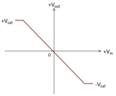
The voltage characteristics, or the transfer curve, of an op-amp is as shown in the figure above. It can be noted that when the input signal VIN is positive, the output VOUT is negative and vice versa. Also, the output changes linearly with respect to input applied. The characteristic curve saturates, or in other words the output becomes a constant, when the input signal amplitude goes beyond the positive and negative power supplies applied to the operational amplifier.
i.e. +VCC = + VSAT and –VCC = -VSAT
Inverting Operational Amplifier Examples
1. Design an inverting amplifier with a gain of -10 and input resistance equal to 10kΩ.
Given are the values of amplifier gain and input resistance.
We know that for an inverting amplifier, ACL = – Rf/R1
Therefore, Rf = -ACL x R1
= – (-10) x 10 kΩ
Rf = 100 kΩ
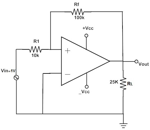
2. In the circuit shown below, R1 = 10 kΩ, Rf = 100 kΩ, Vin = 1V. A load of 25 kΩ is connected to the output terminal. Calculate,
- Current i1
- Output voltage Vout
- Load current iL
(i) Input Current i1
i1 = Vin / R1
= 1 V / 10k Ω
i1 = 0.1 mA
(ii) Output Voltage Vout
Vout = – (Rf / R1) * Vin
= – (100kΩ/10kΩ) x 1 V
Vout = – 10 V
(iii) Load Current iL:
iL = Vout / RL
= 10 V / 25kΩ
iL = 0.4 mA
Trans-Impedance Amplifier
A Trans-impedance amplifier is a simple circuit which converts the input current to the corresponding voltage at the output i.e. it is a current to voltage converter. The trans-impedance amplifier can be used to amplify the current output of photodiodes, photo detectors, accelerometers and other types of sensors to a usable voltage value. The trans-impedance amplifier provides low impedance to the photodiode and isolates it from the output voltage of the op-amp.
A simplest trans-impedance amplifier will have a feedback resistor whose value is very large. The gain of the amplifier is dependent on this resistor. Depending on the application, trans-impedance amplifiers can be configured in various ways. All these different configurations convert the low-level current of a sensor to a significant voltage level. The gain, bandwidth and voltage/current offset values change with different types of sensors.
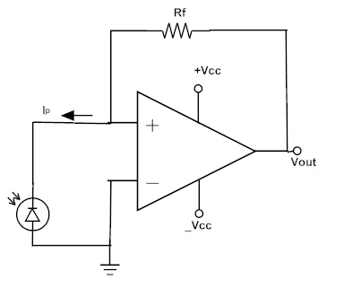
DC Operation
The circuit diagram of a basic trans-impedance amplifier is shown in the above figure. The photodiode is connected to the inverting input terminal. The non-inverting input terminal is connected to ground. This provides a low impedance load for the photodiode, which keeps the voltage across photodiode low. The high gain of the op-amp keeps the photodiode current equal to the feedback current through Rf. Since the photodiode has no external bias in this circuit, the input offset voltage due to the photodiode is very low. This permits a large voltage gain, without any significant output offset voltage.
It can be noted that
-Ip = Vout / Rf
i.e. Vout / Ip = -Rf
The above equation is the DC and low-frequency gain of the trans-impedance amplifier. If the gain is large, any input offset voltage at the non-inverting input of the op-amp will result in an output offset voltage. To minimize these effects, trans-impedance amplifiers are usually designed with FETs at the op-amp input, which have very low input offset voltages.
The frequency response of a trans-impedance amplifier is inversely proportional to the gain set by the feedback resistor Rf. The sensors that are used in these amplifiers usually have more capacitance than an op-amp can handle. This capacitance across the input terminals of the op-amp along with the op-amp internal capacitance, introduce a low pass filter in the feedback path. The low pass filter response of this filter can be characterized as the feedback factor β, which attenuates the feedback signal.
When the effect of this low pass filter is considered, the circuit’s response equation becomes
Vout = – (1p.Rf) / {1 + (1/ AOLβ)}
Where, AOL is the open-loop gain of the op-amp.
At low frequencies the feedback factor β has little effect on the amplifier response. The amplifier response will be close to the ideal value, as long as the open-loop gain (AOLβ)is much greater than unity.
Inverting Amplifier Summary
- An inverting amplifier circuit employs a negative feedback and produces an inverted output with respect to the input. The gain of an inverting amplifier is, thus, indicated as negative.
- The voltage gain of inverting amplifier is independent of the op-amp open-loop gain, which is very large.
- The voltage gain of the inverting amplifier depends upon the resistor values used and hence the gain can be accurately controlled by choosing the values of R1 and Rf appropriately.
- If Rf > R1, the gain will be greater than 1.
- If Rf < R1, the gain will be less than 1.
- If Rf = R1, the gain will be unity.
- Thus, the output voltage can be greater than, less than or equal to the input voltage in magnitude and 180o out of phase.


