An operational amplifier, also called as an op-amp or op amp, is an integrated circuit primarily designed for performing analogue computations. It has a very high voltage gain, typically of the order of 105 (100dB).
Although they are initially designed for performing mathematical operations like addition, subtraction, integration, differentiation etc., (hence the name Operational Amplifiers), by using external components like resistors and capacitors to create a required feedback mechanism, it can also be used as an amplifier and for many other functions like filters, comparators etc.
Op-Amp ICs have become an integral part of almost all analogue circuitry. In this article we will take a look at one of the most used Op-Amp ICs: IC 741 Op Amp.
For learning more about Op-Amps, visit this page: Operational Amplifier Basics
What Is IC 741 Op Amp (Operational Amplifier)?
741 Op Amp IC is a monolithic integrated circuit, comprising of a general purpose Operational Amplifier. It was first manufactured by Fairchild semiconductors in the year 1963. The number 741 indicates that this operational amplifier IC has 7 functional pins, 4 pins capable of taking input and 1 output pin.
IC 741 OpAmp can provide high voltage gain and can be operated over a wide range of voltages, which makes it the best choice for use in integrators, summing amplifiers and general feedback applications. It also features short circuit protection and internal frequency compensation circuits built in it. This Op-amp IC comes in the following form factors:
- 8 Pin DIP Package
- TO5-8 Metal can package
- 8 Pin SOIC
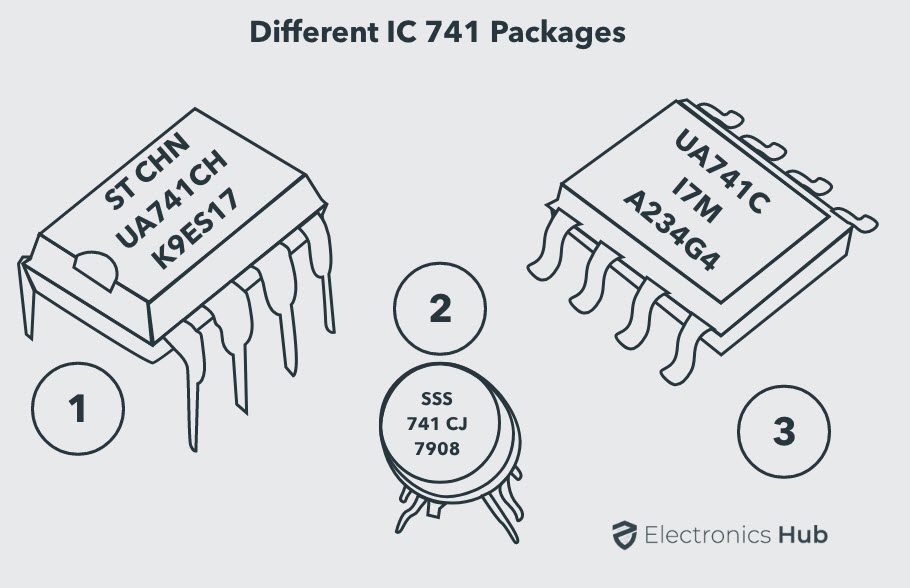
NOTE: The manufacturer of the first IC in the above picture in 8-pin DIP Package is STMicroelectronics and that of the third IC in 8-pin SOIC format is Texas Instruments. We couldn’t find the information on the manufacturer of the second TO5-8 Metal can package IC.
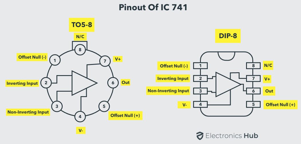
Pinout Of IC 741 Op Amp (Pin Diagram)
An IC 741 op-amp package consists of 8 pins. The below IC 741 Pin Diagram illustrates the pin configurations and internal block diagram of IC 741 in 8 pin DIP and TO5-8 metal can package.
741 IC Op Amplifier Circuit Functions
Now let’s take a look at the functions of different pins of 741 IC op-amp circuits:
- Pin4 & Pin7 (Power Supply): Pin7 is the positive voltage supply terminal and Pin4 is the negative voltage supply terminal. The 741 IC draws in power for its operation from these pins. The voltage between these two pins can be anywhere between 5V and 18V.
- Pin6 (Output): This is the output pin of IC 741. The voltage at this pin depends on the signals at the input pins and the feedback mechanism used. If the output is said to be high, it means that voltage at the output is equal to positive supply voltage. Similarly, if the output is said to be low, it means that voltage at the output is equal to negative supply voltage.
- Pin2 & Pin3 (Input): These are input pins for the IC. Pin2 is the inverting input and Pin3 is the non-inverting input. If the voltage at Pin2 is greater than the voltage at Pin3, i.e., the voltage at inverting input is higher, the output signal stays low. Similarly, if the voltage at Pin3 is greater than the voltage at Pin2, i.e., the voltage at non-inverting input is high, the output goes high.
- Pin1 & Pin5 (Offset Null): Because of high gain provided by 741 Op-Amp, even slight differences in voltages at the inverting and non-inverting inputs, caused due to irregularities in manufacturing process or external disturbances, can influence the output. To nullify this effect, an offset voltage can be applied at pin1 and pin5, and is usually done using a potentiometer.
- Pin8 (N/C): This pin is not connected to any circuit inside 741 IC. It’s just a dummy lead used to fill the void space in standard 8 pin packages.
IC 741 Specifications
The following are the basic specifications of IC 741 operational amplifier:
- Power Supply: Requires a Minimum voltage of 5V and can withstand up to 18V
- Input Impedance: About 2 MΩ
- Output impedance: About 75 Ω
- Voltage Gain: 200,000 for low frequencies (200 V / mV)
- Maximum Output Current: 20 mA
- Recommended Output Load: Greater than 2 KΩ
- Input Offset: Ranges between 2 mV and 6 mV
- Slew Rate: 0.5V/µS (It is the rate at which an Op-Amp can detect voltage changes)
The high input impedance and very small output impedance makes IC 741 a near ideal voltage amplifier.
NOTE: The above mentioned specifications are generic and may vary from manufacturer to manufacturer. To get accurate information, please refer to the datasheet.
Internal Schematic & Working of IC 741
A standard 741 operational amplifier is made up of a circuit containing 20 transistors and 11 resistors. All of them are integrated into a monolithic chip. The below amp op circuit diagram illustrates the internal connections of those components.
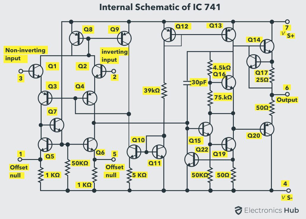
Inverting and non-inverting inputs are connected to two NPN transistors, Q1 & Q2 respectively. Both the transistors behave as NPN emitter followers, with their outputs fed to a pair of PNP transistors Q3 & Q4, which are configured to function as common-base amplifiers. This configuration isolates both the inputs and prevents possible signal feedback that might occur.
Voltage swings at the inputs of Op-Amp can influence the current flow in the internal circuit and it might go beyond the active operation range of any transistor in the circuit. In order to prevent that from happening, two current mirrors are used.
Transistor pairs Q8, Q9 and Q12, Q13 are arranged to form the two current mirror circuits. The transistors Q8 and Q12 are the controlling transistors, which sets the emitter base voltage of the other transistor in the corresponding pair.
This voltage is controlled precisely down to fractions of millivolts in order to allow only the required amount of current to flow. The first current mirror formed by Q8 & Q9 are coupled to the input circuit and the second current mirror formed by Q12 & Q13 are coupled to the output circuit.
A third current mirror formed by the transistors Q10 & Q11 acts as a high-impedance connection between the input circuit and negative of the power supply. It provides a reference voltage without loading the input circuit and sets the slight base bias current required by the PNP transistors at the input common-base amplifier circuit.
Transistor Q6 along with resistors 4.5 KΩ and 7.5 KΩ form a voltage level shifter circuit, which drops the voltage from input amplifier circuit by 1V before it is sent to the succeeding circuit. This is done to prevent signal distortions at the output amplifier stage.
Transistors Q15, Q19 & Q22 are configured to work as a class A amplifier and the transistors Q14, Q17 & Q20 form the output stage of the 741 Operational Amplifier.
To balance any irregularities at the input differential circuit, transistors Q5, Q6 and Q7 are used to form an arrangement that takes in two inputs (Offset null(+), Offset null(-)) and balances both the inverting and non-inverting inputs accordingly.
IC 741 Gain vs Frequency Characteristics
The gain of operational amplifier IC 741 is not constant and varies depending on the frequency of input signal. The below graph illustrates the relation between them:
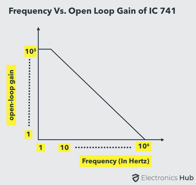
You can observe that the gain remains constant at around 200,000 when the operational amplifier is operated at frequencies below 10Hz. As the frequency of input signal increases, the gain reduces and approaches unity at frequencies around 100,000Hz.
Open Loop Configuration of IC 741
The simplest way to use an operational amplifier is to operate it in the open loop condition.
741 Op Amp Circuits
We will take a look at two different voltage amplifier circuits that use IC 741.
Inverting Amplifier Circuit Using 741 Op Amp
Below is the circuit diagram of an inverting amplifier using 741 IC and two resistors.
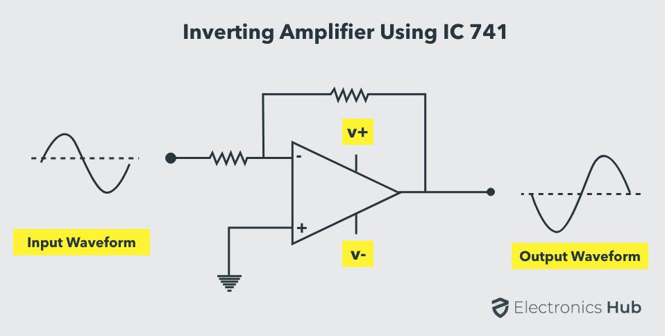
This arrangement is named as inverting because it amplifies and reverses the polarity of input signal (Observe the waveforms at the input and output). Resistor R2 is the feedback resistor. Gain of the amplifier is given by the formula:
Gain (AV) = -(R2 / R1)
Negative sign indicates that the polarity of the output waveform is reversed. By adjusting the values of R1 and R2 desired amplification can be achieved.
Non-Inverting Amplifier Circuit Using 741 Op-Amp
Below is the circuit diagram of a non-inverting amplifier using 741 IC and two resistors.

This arrangement is named as non-inverting because it amplifies the input signal, while retaining the same polarity. Gain of the amplifier is given by the formula:
Gain (AV) = 1 + (R2 / R1)
By adjusting the values of R1 and R2 desired amplification can be achieved.
If the value of feedback resistor R2 is made 0, the gain equals 1 and the Op-Amp configuration behaves as a “unity gain buffer” or a voltage follower.
741 Op-Amp Circuits Applications
Below are the applications of IC 741 Op Amp across different use cases:
-
- Amplifiers: 741 IC is mostly used to amplify signals of varying frequencies ranging from DC to higher radio frequencies. It is also used in frequency selective amplifiers which filter out signals of unwanted frequencies, E.g. tone control systems in stereo and Hi Fi systems.
- Computational: Many electronic circuits that perform mathematical operations like integration, differentiation, summers etc. use 741 Op-Amp.
- Rectifiers: Ordinary diodes used in rectifiers have voltage drop across them which makes it unsuitable for high accuracy signal rectifiers. The 741 IC can be configured to perform as an ideal diode i.e., with no voltage drop at all and can be used in precise rectifier circuits.
- Oscillators: Op-Amp IC 741 is used as an oscillator in function generators to create different output waveforms like sinusoidal, square, triangular etc. It is also used in Pulse Width Modulators (PWM generators)
- Comparators: The 741 IC can be used to compare voltage signals and determine if they are almost of the same voltage. This can be used in voltage regulators and signal comparators.
- ADCs / DACs: 741 Op-Amp can be used to create Digital to Analogue Converters that can take digital binary input from computers or microcontrollers and create a corresponding analogue signal. Similarly, it is can also used in Analogue to Digital circuits.
741 Op Amp Characteristics
Here are the characteristics and features of Op Amp 741 IC:
- High input impedance: Allows for minimal loading of the input signal source.
- Low output impedance: Provides a stable output voltage even with varying loads.
- High voltage gain: Amplifies input signals effectively.
- Wide bandwidth: Can handle a wide range of frequencies.
- Offset voltage and current: Represents the ideal input voltage required to produce zero output voltage.
- Slew rate: Determines the maximum rate of change of the output voltage.
- Common-mode rejection ratio (CMRR): Measures the op-amp’s ability to reject common-mode signals.
- Power supply rejection ratio (PSRR): Indicates how well the op-amp rejects power supply noise.
Conclusion
A complete introduction on IC 741 Op Amp. You learned some basics of Operational Amplifiers, packaging and pinout information of IC 741 Op Amp, important specifications and characteristics, couple of famous circuits using IC 741 (Inverting and Non-Inverting Amplifiers) and some common applications.
FAQs: 741 Op Amp Circuits
1. Why does IC 741 have 8 pins?
Ans: IC 741 op-amp package contains 8 pins to accommodate the two input terminals, one output terminal, power supply terminals, offset null terminals, and ground.
2. What is the difference between IC 555 and IC 741?
Ans: IC 555 is a timer integrated circuit, primarily used for generating time-based waveforms, while IC 741 is an operational amplifier used for amplification, filtering, and other analog signal processing tasks.
3. Are there any disadvantages with IC 741?
Ans: Op Amp IC 741 suffers from limitations such as low slew rate, limited bandwidth, and relatively high offset voltage and current, restricting its use in high-frequency and precision applications.
4. Why is IC 741 not used for high frequency applications?
Ans: IC 741 has a low slew rate, meaning it cannot respond quickly to rapidly changing input signals. This limitation makes it unsuitable for high-frequency applications where fast signal processing is required.
5. What is the alternative to 741 IC?
Ans: Modern op-amps like the LM358, TL072, or op-amps from the 741 family itself (like the LM741CN) offer improved performance in terms of speed, precision, and power consumption compared to the classic 741.
6. How many terminals does IC 741 have?
Ans: An IC 741 op-amp has 8 terminals, which are the connection points for the integrated circuit package.
7. What is the maximum frequency of a 741 op-amp?
Ans: The maximum frequency of a 741 op-amp is typically around 1 MHz, beyond which its performance degrades significantly due to its limited slew rate.

2 Responses
Hai,
I had a doubt with internal circuit working, Inverting and Non inverting terminal input are internally connect to transistor, then how to accept the input (ex:100mV,1mV) below Vfd voltage of transistor .
Great work