A power amplifier circuit is the one with minimum output impedance, used to drive loads like a speaker, which require high power at low impedance. Here we designed a power amplifier circuit using push pull class AB configuration to derive a power of 150W to drive a load of 8 Ohms (speaker).
Principle Behind Power Amplifier Circuit:
The basic principle behind this circuit is the different ways of biasing of a bipolar junction transistor. The electric signal output from a microphone is very low. This low voltage signal is amplified to a sustainable level using the CE configuration of a BJT, biased in class A mode. In this mode, the output is an inverted amplified signal. This signal is a low power signal. Two Darlington power transistors arranged in class AB configuration amplify the power level of this signal. A transistor configured in class A mode is used to drive this transistor.
Related Post – 100W MOSFET Power Amplifier Circuit
Power Amplifier Circuit Theory :
Two important aspects of this circuit are class AB amplifiers and class A voltage amplifiers. A transistor biased in class AB mode produces an amplified output signal for only one half of the input signal. Thus a AB amplifier consists of two matched transistors such that one conducts for one half of the input signal and another conducts for the second half. A practical class AB amplifier consists of diodes to provide biasing to the two transistors, so as to eliminate the cross over distortion. This amplifier is driven by a transistor arranged in common emitter configuration.
A transistor biased in class A mode produces an inverted version of the input signal. However the efficiency is low and so is the output impedance.
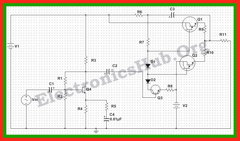
Circuit Diagram of 150W Power Amplifier Circuit:
Power Amplifier Circuit Design:
Design of Class AB Amplifier Stage:
- Selection of Transistors: Here the required output power is 150W. Keeping in mind the power dissipation of transistors, we assume the required power to be about 200W. Here we select +/-50V dual supply, i.e. Vcc = 50V and load is 8Ohms. For better efficiency of the circuit, we select Darlington pair transistors – TIP142(NPN) and TIP147(PNP).
- Selection of Bias Resistor: Voltage across the bias resistor should be about 1.4V less than Vcc. Also since the average collector current is quite large, the biasing current is quite small. Thus large value resistors are used. Here we use resistor of 3K.
- Selection of Diodes:- The two diodes are used to provide proper biasing to the power transistors, so as to eliminate cross over distortion. The diodes should be chosen such that their thermal characteristics are similar to that of the transistors. Here we are using diodes 1N4007.
- Selection of Output Resistors:- Two swamping resistors are used to minimize any difference between the characteristics of the two matched transistors and provide thermal compensation. These resistors should be of low value and here we choose 0.33Ohms.
- Selection of Bootstrap Resistor and Capacitors:- Bootstrapping is done to increase the input impedance of the Darlington transistors. Here we select a electrolyte capacitor of 10uF such that its reactance is less at minimum 20Hz. The value of resistor should be large so as to provide high input impedance. Here we select a resistor of 3K.
Design of Driver Stage:
- Selection of Transistor: Here we select a power transistor TIP41 to provide high power, high gain output.
- Selection of Emitter Resistance: The emitter voltage of the driver transistor is the difference between half of Vcc and Vbe. Since Vcc is 50V and Vbe is 0.7V, we get emitter voltage as 24.3V. Since the emitter current is same as that of quiescent collector current for the transistor, we get the value of resistor Re as around 50Ohms. However here we select a 40Ohms resistor.
- Selection of Coupling Capacitor: The coupling capacitor is used to provide AC signal from the output stage of the preceding amplifier to the input of the driver stage. Here we select a 10uF electrolyte capacitor.
Design of Audio Preamplifier Stage:
- Selection of Transistor: Since here Vcc is around 50V, we select a transistor with maximum open source collector to emitter voltage greater than Vcc. For this purpose NPN transistor BC546 suits our requirement.
- Selection of Load Resistor, R3: The quiescent collector current as seen from the datasheet of BC546 is around 2mA. The value of load resistor is chosen such that when a current of 2mA passes through it, the voltage across it is half of Vcc. This gives the load resistor as 12.5K. Here we select a 10K resistor.
- Selection of Biasing Resistors, R1 and R2: The biasing current is assumed to be 10 times the base current. As small signal gain of BC546 is around 125, the base current is about 0.016mA and the bias current is 0.16mA. Also the base voltage is more than emitter voltage by 0.7V. Assume the emitter voltage, Ve to be 12% of Vcc, i.e. 6V.
This gives,
R1 = (Vcc-Vb)/Ie = 24.5K. Here we select a 25K resistor
R2 = Vb/Ie = 3.35K. Here we select a 3K resistor.
- Selection of feedback resistor,R5: Here we assume the required gain, Av = 50. Since load resistor is about 10K, value of feedback resistor is calculated to be around 200Ohms.
- Selection of emitter resistor, R4: The total emitter resistor value is given by Ve/Ie, i.e. 3K. However since this resistor is shared with the feedback resistor, the emitter resistor is around 3K-200 = 2.8K. Here we select a 2K resistor.
- Selection of emitter capacitor: The value of this capacitor should be such that the reactance is less than the total emitter resistance. Here we select a 0.01uF electrolyte capacitor.
- Selection of coupling capacitor: The coupling capacitor is an electrolyte capacitor of 10uF.
Testing the Power Amplifier Circuit:
Once the circuit is designed and drawn on Multisim, the input is given by connecting a AC signal voltage source to the coupling capacitor of the preamplifier stage. The input is set at 4Vpp, 1kHz. The output is determined by connecting a Wattmeter such that voltage terminals are connected across the load resistor of 8Ohms and the current terminals are connected between the output terminal and the load resistor. Here we observe the maximum output power to be around 200W.
Related Post – 100w Subwoofer Amplifier Circuit
Applications of Power Amplifier Circuit:
- This circuit can be used to drive a loudspeaker of low input impedance, in audio amplification.
- We can also use this circuit to drive high power antennas for long range transmission.
Limitations:
- This circuit is theoretical and the output contains distortion.
- The use of linear devices like BJTs cause more power dissipation, thus reducing the efficiency of the system.

5 Responses
It’s really good concept.looking easy.
How can i design this to have an output of 100w
How can i design this to have an output of 250w
Can I use TIP122 instead of TIP141, and is the AC source “Function generator” necessary. I am trying to make a loudspeaker that I can carry out with me XD
Thanx very much for the circuit, I will try it.