Digital signals are processed by the digital system which can be built with various logic gates. These logic circuits are made of various logic gates , by connecting them in certain combinations , in order to produce the required output. Digital logic circuits are mainly classified into two types , sequential logic circuits and combinational logic circuits. This article gives a brief idea about the combinational logic circuits.
Combinational Logic Circuits
A combinational logic circuit is one in which the present state of the combination of the logic inputs decides the output . The term combination logic means combining of two or more logic gates to form a required function where the output at a given time depends only on the input.
The logic gates are the fundamental building blocks of a combinational circuit. By using the combination of logic gates more complex combinational circuits can be implemented such as multiplexers and de-multiplexers, comparators, adders and subtractors, etc.
A combinational circuit comprises of input variables, logic gates and output variables. The logic gates accepts the inputs and depending on the type of functioning of the logic gate,output signals are generated from them.
The required output data is obtained from this process by transforming the binary information given at the input. The figure below shows the schematic representation of a generalized combinational logic circuit consisting of n input variable and m output variables.
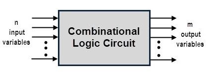
In the above figure, there are n input variables and hence there will be 2n possible combinations of bits at the input. By a Boolean expression of input variables, each output is expressed. So the result of above generalized combinational logic circuit can be expressed by m Boolean expressions.
In the above figure, the circuit accepts the binary variables and depending on the logical combination of gates it generate outputs.
Design Procedure of Combinational Logic Circuits
A combinational circuit can be designed using the following steps.
- Identification and determination of number of available input variables and required output variables.
- Representing symbols (alphabets) for each and every input and output variables.
- Expressing the input and output variable’s relationship.
- Construction of truth table indicating the relationship between the input and output variables.
- Obtaining the Boolean expression for each output variable in terms of input variables.
- Minimizing the Boolean expressions of various output variables.
- Obtaining the logic diagram by the implementation of minimized Boolean expressions.
For minimizing Boolean expressions, various simplification techniques are available so that they reduce the number of gates, hence less implementation cost. These techniques include Boolean algebra theorems and identities, Karnaugh maps (K-maps), Quinne-McCluskey tabulation, etc. For hardware implementation of the combinational circuit, the following guidelines are mostly preferred.
- The implementation of the circuit should be in such that , it should have minimum number of gates, having a minimum number of inputs.
- The number of interconnections between the gates should be minimum and the propagation time should be shortest.
- There should be always a limitation on the driving capability of the gates.
This is the simple, effective and traditional method of designing a combinational circuit for small circuit. If the circuit is more complex, number of gates required is more and also it requires more number of wires in between them. Hence, designing such circuits may be less reliable and time consuming.
To overcome these problems, most of the combinational circuits are available in integrated circuits (ICs) which are extensively used in the design of the digital systems. Depends on the integration capability of gates, these ICs are classified into small, medium, large and very large scale ICs.
For performing specific digital functions such as addition, multiplexing, de-multiplexing, encoding, decoding, comparison, etc., mostly medium scale integrated (MSI) ICs are used in digital systems.
Example of Combinational Logic Circuit
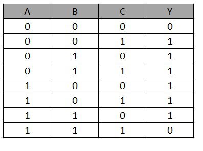
Statement: Design a combinational logic circuit with three input variables such that it will produce logic 1 output when one or two the input variables are logic 1 but not all the three.
Solution: Follow the above listed points to design the logic diagram as per the given statement. In the given statement there are three input variables and one output variable. As a second step, assign the input variables with letter symbols as A, B, C and output as Y. Next, the relationship between the input and output variables can be tabulated by constructing the truth table as given below.
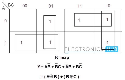
Now, the simplified Boolean expression for the above truth table for getting the output Y is obtained by using K-map simplification as
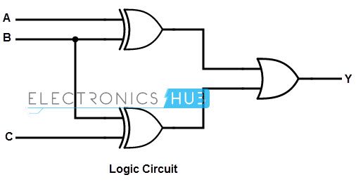
By implementing the above Boolean equation we get the logic diagram as
Classification of Combinational Logic Circuits
Combinational circuits are used in a wide variety applications including calculators, digital measuring techniques, computers, digital processing, automatic control of machines, industrial processing, digital communications, etc.
Different types of combinational logic circuits are used for various applications.Depending on the function of the logic circuit employed for, combinational logic circuits are mainly classified into three types, namely Arithmetic and logic circuits, data transmission circuits and code converter circuits.
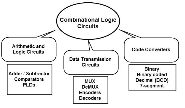
Arithmetic and Logic Circuits
Arithmetic operations are one of the main functionalities of most computers and calculators. These operations are carried by the logic gates or simply combinational circuits which combines the several logic gates to perform the required function. These arithmetic functionalities of the combinational circuits include addition, subtraction, multiplication, etc.
Some of the combinational circuits used for these operations are Half- adder, Full-adder, Half-subtractors, Full subtractors, Adder-subtractors, Comparators, PLDs (Programmable Logic Devices), etc.
Data Transmission Circuits
The most commonly used combinational circuits are multiplexers and de-multiplexers. A multiplexer logic circuit accepts the several data inputs and passes one of them through the output at a time. These are used in data selection, parallel to series conversion, data routing applications in digital systems.
A de-multiplexer circuit performs the reverse operation than that of the multiplexer. It accepts the single input and distributes it to multiple outputs. These are used in distributors as well as series to parallel converter applications.
Other essential data transmission circuits include encoders and decoders. A decoder logic circuit converts n-bit binary input code into 2n output lines. Each output line is activated for only one of the possible combinations of the inputs.
These are used in data de-multiplexing, digital to analog converters and digital display applications. An encoder digital circuit converts an active input signal into a coded output signal as reverse operation of the decoder. These are used in bit compression applications.
Code Converter Circuits
In some applications, it is required to interface two digital blocks of different coding systems. So a conversion circuit is used in between such circuits to convert the information. Some of these converters are binary to gray code, gray to binary, BCD to excess-3 code, Excess-3 to BCD code and seven segment code converter circuits.
