In this tutorial, we will learn about CMOS Technology, what are the advantages of CMOS Technology, basic working a simple CMOS Inverter and a few logic gates like NAND and NOR that are implemented using CMOS.
Introduction
CMOS, which is short for Complimentary Metal-Oxide Semiconductor, is a predominant technology for manufacturing integrated circuits. This dominance of CMOS Technology in the fabrication of Integrated Circuits or ICs will continue for decades to come.
Generally, the CMOS Technology is associated with VLSI or Very Large-Scale Integrated Circuit, where a few millions or even billions of transistors (MOSFETs to be specific) are integrated into a single chip or die.
The reasons for the dominant use of CMOS Technology in the fabrication of VLSI chips are reliability, low power consumption, considerably low cost and most importantly scalability.
You might have heard of the famous Moore’s Law described by Gordan Moore, according to whom, the number of devices on a chip will double every 18 to 24 months. Even though Gordan Moore did not imply it to CMOS, the Moore’s Law been successfully fulfilled due to the CMOS technology.
Today, we are dealing with channel lengths as small as 7nm (at the time of publishing this tutorial), all because of the scaling ability in CMOS.
Logic Families
Before going into more details of CMOS, let us briefly understand what are logic families. Integrated Circuit or chip is a device that has number of circuits integrated as one entity. Since IC is a way simplify the complexity, there are many types of circuit configurations that are used in the production if integrated circuits.
All these circuit configuration approaches are known as Logic Families. The idea behind logic families is that different logic functions of a circuit when fabricated as an IC that are put together using a single approach will have same electrical characteristics.
Some of these characteristics are power dissipation, power supply, speed, noise etc.
As most of the ICs are manufactured using either Bipolar Devices or MOS Device, the logic families are also divided into two families: The Bipolar families and the MOS families.
Bipolar Logic Families
The following is a list of the Bipolar Logic Families.
- Diode Logic (DL)
- Resistor Transistor Logic (RTL)
- Diode Transistor Logic (DTL)
- Transistor Transistor Logic (TTL)
- Emitter Coupled Logic (ECL)
- Integrated Injection Logic (I2L)
MOS Logic Families
The following is a list of the MOS Logic Families.
- PMOS Family (uses p-Channel MOSFET)
- NMOS Family (uses n-Channel MOSFET)
- CMOS Family (uses both p-Channel MOSFET and n-Channel MOSFET)
There is another logic family called Bi-CMOS Family which uses both Bipolar devices as well as MOS devices.
PMOS and NMOS Technologies
Before the extensive use of CMOS Technology for implementing logic gates and in fabrication of ICs, PMOS and NMOS logic were widely used. In fact, the Intel 4004 and the initial version of Intel 8008 are fabricated using PMOS technology.
PMOS was later replaced by the NMOS technology, which is one of the widely used IC Fabrication technologies (before CMOS). Initially, even CMOS was slower and expensive than NMOS.
NMOS became the “standard process” for integrated circuits. The main advantages of NMOS technology are simple physical process, high functional density, good speed (initially faster than CMOS) and easier to manufacture.
The main drawbacks of NMOS technology are its electrical asymmetry and static power dissipation. All these drawbacks are minimized by the CMOS Technology.
CMOS Technology
The CMOS Technology uses both NMOS and PMOS to realize various logic functions. Both the N-channel MOSFET and the P-channel MOSFET are design in such a way that they have matching characteristics (during ON and OFF state).
The main advantage of CMOS technology over Bipolar or the previous popular NMOS technologies is its extremely low power consumption in static conditions as they draw power only during switching operation.
This allows integrating much larger number of logic gates on the VLSI IC when compared to Bipolar or NMOS technologies.
Today, CMOS technology is the dominant IC fabrication technology in VLSI industry and is used for making high end microprocessors, microcontroller, memory modules, sensors and Application Specific Integrated Circuits (ASICs).
The combination of NMOS and PMOS devices in a CMOS logic makes it easier to design different logic functions. With the improvements in CMOS IC fabrication technologies, the size of the transistor can be scaled down in size.
Downscaling the size of the transistor implies that more logical functions can be integrated into the same IC without compromising the speed and power.
Initially, the CMOS IC Technology was used in the fabrication of Digital Logic ICs. The development towards low cost and increased functionality has led to CMOS technology being used in Analog ICs and Mixed Signal Designs.
CMOS Logic
Static CMOS circuits consists of combinational logic gates with one or more inputs and one output. Let us see a few important CMOS Logic gates.
Inverter
The simplest of the logic gates is the Inverter. It is an essential part of digital design and understanding the operation and properties of an Inverter will make it significantly easier to study NAND Gates, Adders, Multiplexers and even Microprocessors.
Following is the circuit of a CMOS Inverter Gate along with its symbols.
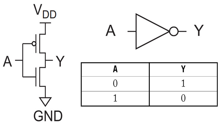
CMOS Inverter is also known as the NOT Gate. From the above circuit, you can see that a CMOS Inverter consists of an N-channel MOSFET (NMOS) and a P-channel MOSFET (PMOS).
When the input A is LOW i.e. Logic 0, the NMOS Transistor is OFF and the PMOS Transistor is ON. The P-channel MOSFET provides a path for the VDD to appear at the Output. Hence, the output is HIGH i.e. Logic 1.
Similarly, when the input is HIGH, NMOS is ON and PMOS is OFF. The output is connected to GND and the output is LOW.
NAND
The following circuit shows a 2-input CMOS NAND Gate. As seen in the image, a 2-input NAND gate consists of two N-channel MOSFETs connected in series between output and GND and two P-channel MOSFETs connect in parallel between VDD and output.
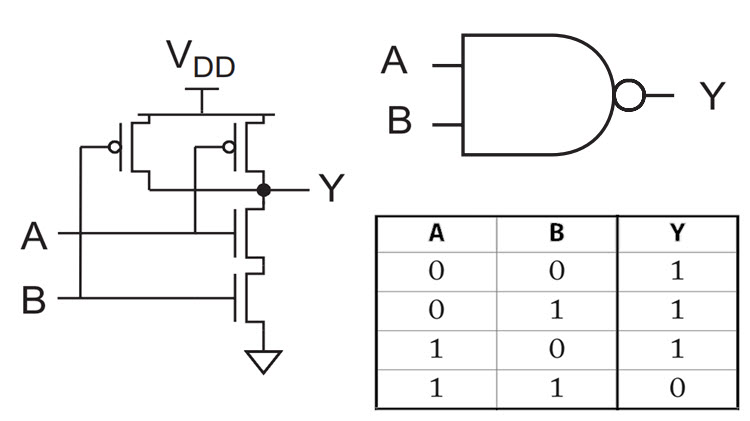
When any of the inputs A or B is LOW, atleast one of the NMOS Transistors will be OFF. For the output to be LOW, both the inputs should be HIGH. For all the other combinations of the inputs, the output will be HIGH.
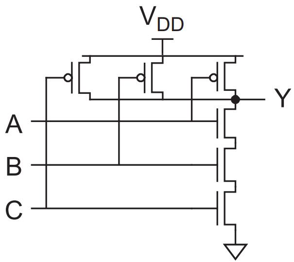
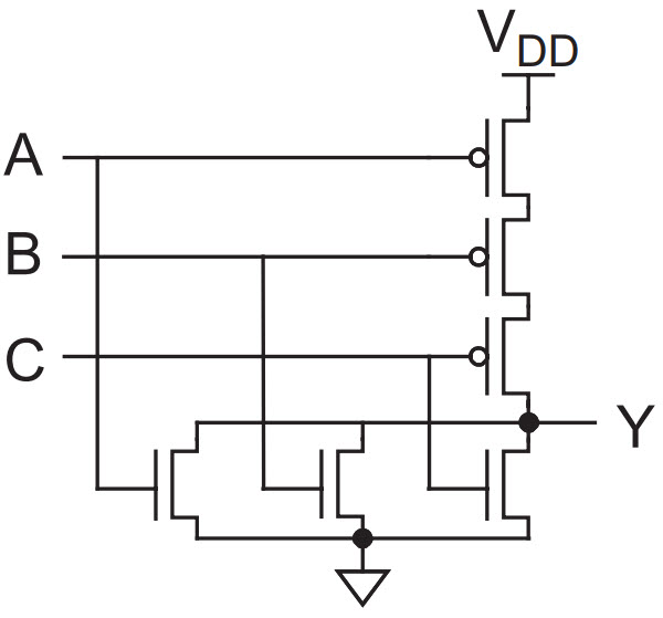
Based on the same principle as a 2-input NAND gate, a 3-input CMOS NAND Gate cam be designed, where there are 3 NMOS Transistors in series between output and GND and 3 PMOS Transistors in parallel between VDD and output.
NOR
Circuit of a 2-input CMOS NOR Gate is shown below. It consists of two P-channel MOSFETs connected in series between VDD and Output and two N-channel MOSFETs connected in parallel between Output and GND.
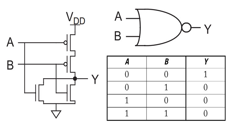
When either of the inputs A or B is HIGH, the output is LOW as atleast one NMOS Transistor is ON. For the output to be HIGH, both the inputs must be LOW.
Similar to the 3-input NAND gate, a 3-input NOR gate can also be designed as shown in the following circuits.
Principle behind CMOS Logic
The name complementary in CMOS refers to the fact that both NMOS and PMOS Transistors are used in the same design. The main principle behind a CMOS logic gate is that the NMOS Transistors act as Pull-down network to connect Output to GND and the PMOS Transistors act as Pull-up network to connect VDD to Output.
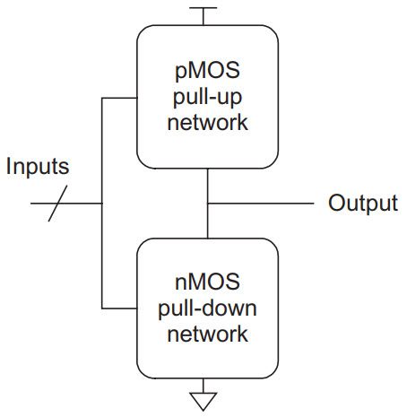
CMOS logic is arranged in such a way that only one of the pull-up or pull-down networks is ON while the other is OFF with the help of a single input.
CMOS Fabrication Technologies
Basically, there are four different processes in which a typical CMOS VLSI IC is manufactured. They are:
- P-Well Process
- N-Well Process
- Twin Tub Process
- Silicon on Insulator (SOI) Process
