Majority of modern communication is Digital in nature i.e., it is a combination of 1’s and 0’s. The digital data is transmitted either through wires (in case of wired communication) or wireless. Even in an advanced mode of communication, there will be errors while transmitting data (due to noise).
The simplest of errors is corruption of a bit i.e., a 1 may be transmitted as a 0 or vice-versa. To confirm whether the received data is the intended data or not, we should be able to detect errors at the receiver. In this tutorial, we will learn about Parity Bit, Even Parity, Odd Parity, Parity Generator, and Parity Checker with a practical example and practical circuit.
What Is Parity Bit?
A parity bit is a basic way to check for errors in digital communications and data storage, used to make sure data stays accurate. It’s an extra binary digit that can be added to a string of binary code. In digital systems, when binary data is transmitted and processed, data may be subjected to noise so that such noise can alter 0s (of data bits) to 1s and 1s to 0s.
Hence, a Parity Bit is added to the word containing data in order to make number of 1s either even or odd. The message containing the data bits along with parity bit is transmitted from transmitter to the receiver. At the receiving end, the number of 1s in the message is counted and if it doesn’t match with the transmitted one, it means there is an error in the data. Thus, the Parity Bit it is used to detect errors, during the transmission of binary data.
Even Parity And Odd Parity
The sum of the data bits and parity bits can be even or odd.
Even Parity:
The parity bit is adjusted so that the total number of 1s in the code, including the parity bit, is even. If there are already an even number of 1s, the parity bit is 0. If there are an odd number of 1s, the parity bit is 1.
Odd Parity:
The parity bit is adjusted to make the total number of 1s odd. If there are already an odd number of 1s, the parity bit is 0. If it’s even 0, the parity bit is set to 1. All those error detection and correction can be done by using Ex-OR gates (since Ex-OR gate produce zero output when there are even number of inputs).
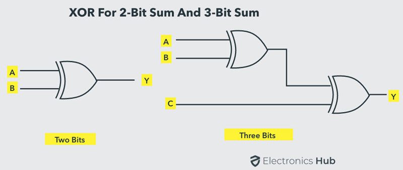
To produce two bits sum, one Ex-OR gate is sufficient whereas for adding three bits, two Ex-OR gates are required as shown in below figure.
Parity Generator Circuit
A parity generator circuit is a combinational logic circuit that is used at the transmitting end. Its primary function is to calculate and add the parity bit to the data stream based on the chosen parity scheme (even or odd).
- The circuit takes the original data stream (e.g., a byte) as input.
- It performs operations on the data bits based on the chosen scheme (even or odd parity).
- Commonly used logic gates for these operations include XOR (exclusive OR).
- The output of the circuit is the original data stream with the appended parity bit
Parity Checker Circuit
A parity checker circuit resides at the receiving end. Its role is to verify the parity of the received data stream (including the parity bit) and detect any potential errors.
- The circuit receives the entire data stream with the parity bit.
- It performs the same calculations on the received data (including the parity bit) as the parity generator did at the transmitter (based on the known even or odd parity scheme).
- It compares the calculated parity with the received parity bit.
Error Detection:
- If the calculated parity matches the received parity bit, it indicates a high probability that the data hasn’t been corrupted during transmission.
- If the calculated parity doesn’t match the received parity bit, it’s a strong indication of a possible single-bit error in the data stream.
Important Note: While parity checking is effective for detecting single-bit errors, it cannot pinpoint the exact location of the error in the data stream. It simply flags the possibility of an error.
Now let us understands what is a parity generator and checker in digital electronics along with the truth tables and formulas.
What Is A Parity Generator?
Parity Generator in digital electronics is a combinational circuit that accepts an n-1 bit data and generates the additional bit that is to be transmitted with the bit stream. This additional or extra bit is called as a Parity Bit.
In even parity bit scheme, the parity bit is ‘0’ if there are even number of 1s in the data stream and the parity bit is ‘1’ if there are odd number of 1s in the data stream.
In odd parity bit scheme, the parity bit is ‘1’ if there are even number of 1s in the data stream and the parity bit is ‘0’ if there are odd number of 1s in the data stream. Let us discuss both even and odd parity generators.
Even Parity Generator
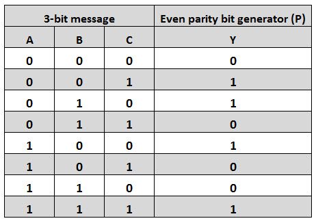
Let us assume that a 3-bit message is to be transmitted with an even parity bit. Let the three inputs A, B and C are applied to the circuit and output bit is the parity bit P. The total number of 1s must be even, to generate the even parity bit P.
Even Parity Checker Truth Table
The figure below shows the 3 bit truth table of even parity generator in which 1 is placed as parity bit in order to make all 1s as even when the number of 1s in the truth table is odd.
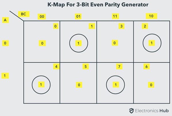
The K-map simplification for 3-bit message even parity generator is
From the above parity checker truth table, the simplified expression of the parity bit can be written as
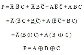
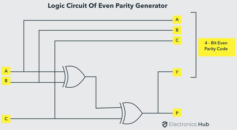
The above expression can be implemented by using two Ex-OR gates. The logic diagram of even parity generator with two Ex – OR gates is shown below. The three bit message along with the parity generated by this circuit which is transmitted to the receiving end where parity checker circuit checks whether any error is present or not.
To generate the even parity bit for a 4-bit data, three Ex-OR gates are required to add the 4-bits and their sum will be the parity bit.
Odd Parity Generator
Let us consider that the 3-bit data is to be transmitted with an odd parity bit. The three inputs are A, B and C and P is the output parity bit. The total number of bits must be odd in order to generate the odd parity bit.
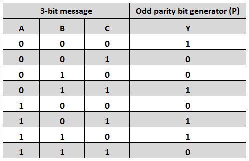
Odd Parity Checker Truth Table
In the given truth table below, 1 is placed in the parity bit in order to make the total number of bits odd when the total number of 1s in the truth table is even.
The truth table of the odd parity generator can be simplified by using K-map as
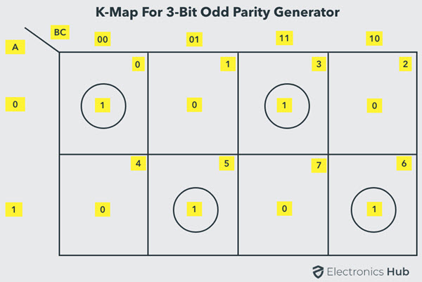
The output parity bit expression for this generator circuit is obtained as
P = A ⊕ (B ⊕ C)
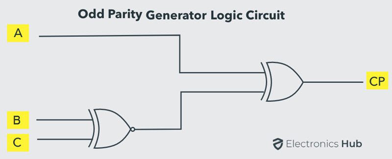
The above Boolean expression can be implemented by using one Ex-OR gate and one Ex-NOR gate in order to design a 3-bit odd parity generator.
The logic circuit of this generator is shown in below figure, in which two inputs are applied at one Ex-OR gate, and this Ex-OR output and third input is applied to the Ex-NOR gate, to produce the odd parity bit. It is also possible to design this circuit by using two Ex-OR gates and one NOT gate.
What Is A Parity Checker?
Parity Checker is a logic circuit that checks for possible errors in the transmission. This circuit can be an even parity checker or odd parity checker depending on the type of parity generated at the transmission end. When this circuit is used as even parity checker, the number of input bits must always be even.
Even Parity Checker
Consider that three input message along with even parity bit is generated at the transmitting end. These 4 bits are applied as input to the parity checker circuit, which checks the possibility of error on the data. Since the data is transmitted with even parity, four bits received at circuit must have an even number of 1s.
If any error occurs, the received message consists of odd number of 1s. The output of the parity checker is denoted by PEC (Parity Error Check).
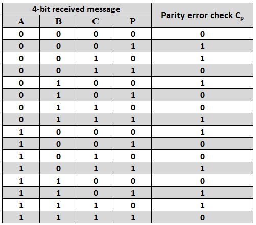
Even Parity Checker Truth Table
The below table shows the truth table for the Even Parity Checker in which PEC = 1 if the error occurs, i.e., the four bits received have odd number of 1s and PEC = 0 if no error occurs, means, if the 4-bit message has even number of 1s.
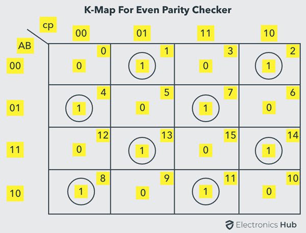
The above truth table can be simplified using K-map as shown below.
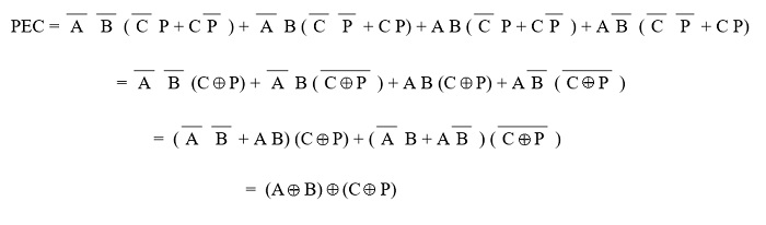
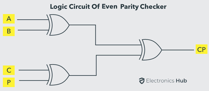
The above logic expression for the even parity checker can be implemented by using three Ex-OR gates as shown in figure. If the received message consists of five bits, then one more Ex-OR gate is required for the even parity checking.
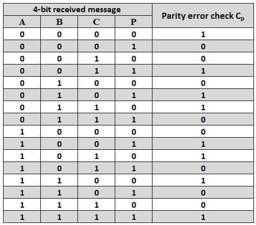
Odd Parity Checker
Consider that a three bit message along with odd parity bit is transmitted at the transmitting end. Odd parity checker circuit receives these 4 bits and checks whether any error are present in the data.
If the total number of 1s in the data is odd, then it indicates no error, whereas if the total number of 1s is even then it indicates the error since the data is transmitted with odd parity at transmitting end.
Odd Parity Checker Truth Table
The below figure shows the truth table for odd parity generator where PEC =1 if the 4-bit message received consists of even number of 1s (hence the error occurred) and PEC= 0 if the message contains odd number of 1s (that means no error).
The expression for the PEC in the above truth table can be simplified by K-map as shown below.
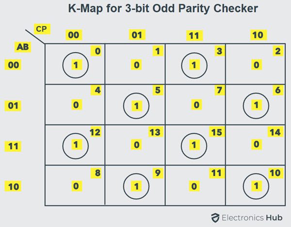
After simplification, the final expression for the PEC is obtained as
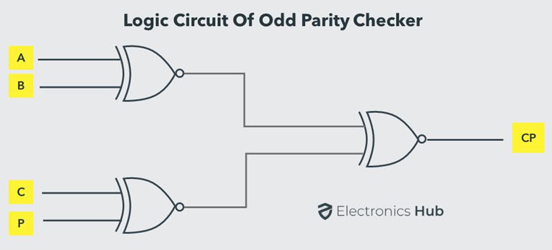
PEC = (A Ex-NOR B) Ex-NOR (C Ex-NOR P)
The expression for the odd parity checker can be designed by using three Ex-NOR gates as shown below.
Parity Generator/Checker ICs
There are different types of parity generator /checker ICs are available with different input configurations such as 5-bit, 4-bit, 9-bit, 12-bit, etc. One of the most commonly used and standard type of parity generator/checker IC is 74180.
It is a 9-bit parity generator or checker used to detect errors in high speed data transmission or data retrieval systems. The figure below shows the pin diagram of 74180 IC.
This IC can be used to generate a 9-bit odd or even parity code or it can be used to check for odd or even parity in a 9-bit code (8 data bits and one parity bit).
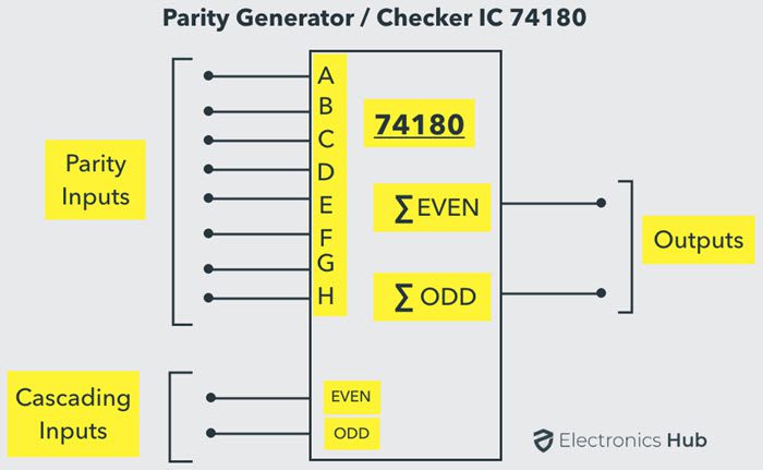
This IC consists of eight parity inputs from A through H and two cascading inputs. There are two outputs even sum and odd sum. In implementing generator or checker circuits, unused parity bits must be tied to logic zero and the cascading inputs must not be equal.
If this IC is used as an Even Parity Checker and when a parity error occurs, the ‘sum even’ output goes low and ‘sum odd’ output goes high. If this IC is used as an Odd Parity Checker, the number of input bits should be odd, but if an error occurs the ‘sum odd’ output goes low and ‘sum even’ output goes high.
FAQs:
How does parity checking work to detect errors?
Parity bits are used for error detection by adding an extra bit to a data block. This extra bit is calculated to make the total number of 1s in the data block either even or odd (depending on the parity scheme). When the data is received, the parity is recalculated. If it doesn’t match the original parity, an error is detected.
What are the differences between odd parity and even parity?
The primary difference between odd and even parity lies in the desired outcome of the parity bit. Odd parity requires an odd number of 1s, even parity requires an even number of 1s.
Which logic gate is a parity checker?
XOR (Exclusive OR) gate is commonly used for parity checking due to its ability to determine if two inputs are different.
How to design a 3 bit even parity generator using logic gates?
A 3-bit even parity generator produces a parity bit based on three input bits (A, B, C). The parity bit is set to 1 if the number of 1s in the input is odd, and 0 if the number of 1s is even. To achieve this, we can use XOR gates. The XOR gate outputs 1 if the inputs are different, and 0 if they are the same.
What is the work of 3 bit parity checker?
A 3-bit parity checker verifies the accuracy of received data. It calculates the parity of the incoming 3 data bits and the received parity bit. If the calculated parity matches the received parity, there’s likely no error. Otherwise, it indicates a potential error in the transmitted data.
How to implement a 4-bit parity generator circuit?
To implement a 4-bit parity generator circuit, use XOR gates to sequentially combine the input bits. The final XOR gate output is the parity bit. Here is the process to implement the 4 bit parity generator:
- Connect input bits A and B to the first XOR gate.
- Connect input bits C and D to the second XOR gate.
- Connect the outputs of the first two XOR gates to the inputs of the third XOR gate.
- The output of the third XOR gate is the parity bit.
What is the parity bit card trick?
A magic trick based on the concept of parity. By manipulating the number of black cards in rows and columns, a magician can seemingly predict which card has been flipped.
What is the simple parity check code?
A basic error detection method that appends a parity bit to data. The parity bit is set to ensure an even or odd number of 1s in the data block.

18 Responses
Superb..!!!! All informations are covered….
awesome…
awesom nd tq
it is covered all topic.it is very help full for me.
nice and usefull
Is exnor or exor or both In the odd parity generator. It is confusing with sentence and figure
tell some important applications
if it is said to design a parity generator to generate an odd parity for four bit word does that mean the parity generator is of 5 bit
Odd Parity Generator diagram is wrong. Correct it ….Look at equation and then at Diagram..
And Thanks for the notes. Appreciate.
There is a huge,mistake, The figure for odd parity generator is actually odd parity checker.
Thank you superb knowledge shared
can u post the difference between parity checker and parity generator
For 4 bit parity generator which ic is required and it’s circuit dig plzz tell me
Not bad
Sir plz present proper applications of parity
nice explanation
For 4 bit parity generator which ic is required ?
Thank you very much