Most often seven-segment displays are used to display the digits in digital watches, calculators, clocks, measuring instruments and digital counters, etc. Generally, LED and LCD segments provide the display output of numerical numbers and characters.
However to display the characters and numbers (in order to produce the decimal readout), seven-segment displays are most commonly used. Mostly these displays are driven by the output stages of digital ICs (to which the visual indication of the output stages has to be performed) such as latches and decade counters, etc.
But these outputs are in the form of 4-bit binary coded decimal (BCD), and not suitable for directly driving the seven-segment displays.
A display decoder is used to convert a BCD or a binary code into a 7 segment code. It generally has 4 input lines and 7 output lines. Here we design a simple display decoder circuit using logic gates.
Even though commercial BCD to 7 segment decoders are available, designing a display decoder using logic gates may prove to be beneficial from economical as well as knowledge point of view.
Principle of Display Decoder Circuit
The basic idea involves driving a common cathode 7-segment LED display using combinational logic circuit. The logic circuit is designed with 4 inputs and 7 outputs, each representing an input to the display IC. Using Karnough’s map, logic circuitry for each input to the display is designed.
Related Post: Water Level Indicator using AVR Microcntroller
Theory Behind the Circuit:
The first and foremost aspect of this circuit is decoder. A decoder is a combinational circuit which is used to convert a binary or BCD (Binary Coded Decimal) number to the corresponding decimal number . It can be a simple binary to decimal decoder or a BCD to 7 segment decoder.
Another relevant section is the combinational logic circuitry. A combinational logic circuit is a system of logic gates consisting of only outputs and inputs. The output of a combinational logic circuit depends only on the present state of the inputs and nothing else. Best examples of such circuits are Encoders and Decoders, Multiplexers and De-multiplexers, Adders, Subtractors etc.
To understand the design and operation of these logic circuits, one needs to have a good knowledge about Boolean algebra and logic gates. For example few basic Boolean algebra rules to be followed are the complementary law, associative law, De-Morgan’s law etc.
A 7 segment LED display consists of an arrangement of 8 LEDs such that either all the anodes are common or cathodes are common. A common cathode 7 segment display consists of 8 pins – 7 input pins labeled from ‘a’ to ‘g’ and 8th pin as common ground pin.
7 Segment Display Decoder Circuit Design
Step 1: The first step of the design involves analysis of the common cathode 7-segment display. A 7-segment display consists of an arrangement of LEDs in an ‘H’ form. A truth table is constructed with the combination of inputs for each decimal number. For example, decimal number 1 would command a combination of b and c (refer the diagram given below).
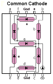
Image Resource Link: www.thelearningpit.com
Step 2: The second step involves constructing the truth table listing the 7 display input signals, decimal number and corresponding 4 digit binary numbers.
BCD To 7 Segment Decoder Truth Table
The truth table for the decoder design depends on the type of 7-segment display. As we mentioned above that for a common cathode seven-segment display, the output of decoder or segment driver must be active high in order to glow the segment.
The figure below shows the truth table of a BCD to seven-segment decoder with common cathode display. In the truth table , there are 7 different output columns corresponding to each of the 7 segments.
Suppose the column for segment a shows the different combinations for which it is to be illuminated. So ‘a’ is active for the digits 0, 2, 3, 5, 6, 7, 8 and 9.
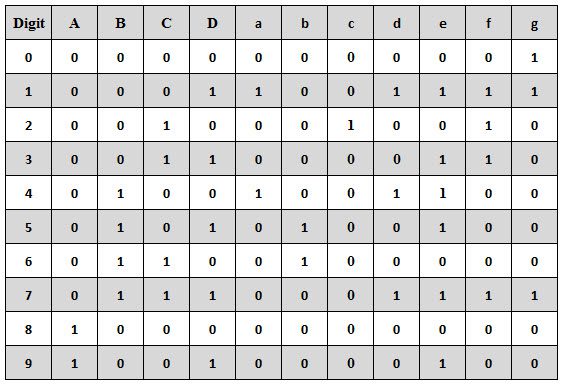
From the above truth table, the 7 Segment Display Boolean expression of each output functions can be written as
a = F1 (A, B, C, D) = ∑m (0, 2, 3, 5, 7, 8, 9)
b = F2 (A, B, C, D) = ∑m (0, 1, 2, 3, 4, 7, 8, 9)
c = F3 (A, B, C, D) = ∑m (0, 1, 3, 4, 5, 6, 7, 8, 9)
d = F4 (A, B, C, D) = ∑m (0, 2, 3, 5, 6, 8)
e = F5 (A, B, C, D) = ∑m (0, 2, 6, 8)
f = F6 (A, B, C, D) = ∑m (0, 4, 5, 6, 8, 9)
g = F7 (A, B, C, D) = ∑m (2, 3, 4, 5, 6, 8, 9)
Step 3: The third step involves constructing the Karnough’s map for each output term and then simplifying them to obtain a logic combination of inputs for each output.
7 Segment Display K Map Simplification
The below figures shows the 7 Segment K map simplification for the common cathode seven-segment decoder in order to design the combinational circuit.
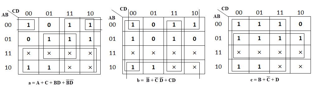
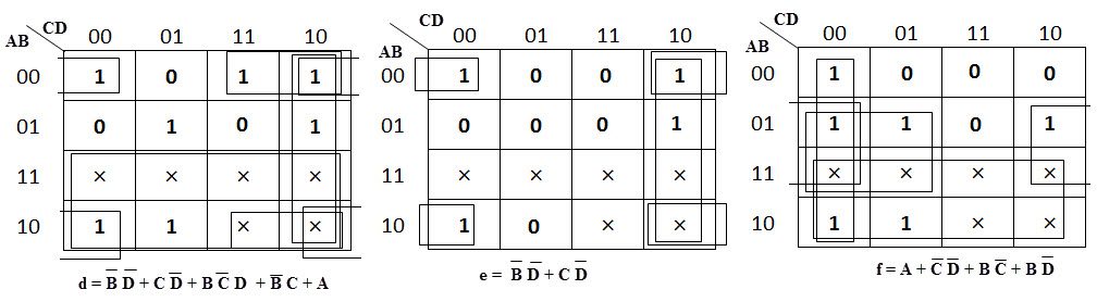
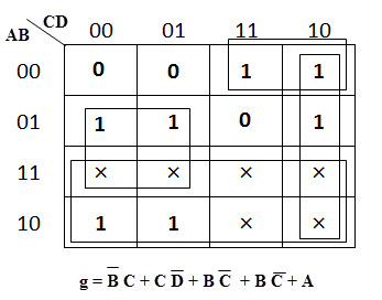
From the above simplification, we get the output values as

Step 4: The final step involves drawing a combinational logic circuit for each output signal. Once the task was accomplished, a combinational logic circuit can be drawn using 4 inputs (A,B,C,D)and a 7- segment display (a,b,c,d,e,f,g) as output.
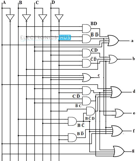
Display Decoder Circuit Operation
The circuit operation can be understood through the truth table itself. When all the inputs are connected to low logic , the output of the combinational logic circuit would be so as to drive all the output LEDs except ‘g’ to conduction. Thus the number 0 will be displayed. Similar operation would take place for all other combinations of the input switches.
Note: Also read the interesting post – LED Blinking Circuits
Practically BCD to 7 segment decoders are available in form of integrated circuits such as 74LS47. Apart from regular 4 input pins and 7 output pins, it consists of a lamping test pin used for segment testing, ripple blanking input pin used to blank off zeros in multiple display systems, ripple blanking output pin used for cascading purposes and a blanking input pin.
Applications of Display Decoder Circuit
- This circuit can be modified using timers and counters to display the number of clock pulses.
- This circuit can be modified to develop an alphabet display system instead of a decimal number display system.
- It can be used as a timer circuit.
[Also Read: How To Make an Adjustable Timer ]
Limitations of Display Decoder Circuit
- This circuit involves lot of logic gates and is quite complex.
- Timing delay by each logic gate is a matter of concern and this circuit might not produce accurate results when used to display count of pulses.
- This is a theoretical circuit and may require few modifications.

39 Responses
it is so help full for our project,,,,,
You may want to double check you Boolean algebra on some of the k-maps. Especially for c, because you have;
c = B + C’ + D
I get from the k-map
c = B + C’D
c = B + C’ + D is correct
Your may be wrong
K-map for b is wrong. m(1) mistakenly became a zero in the map.
The truth table is for a common anode display where logic low enables the segment.
You are right…
is ther k-map of the e right?? the 1001 should be a 0
Your sum of minterms for b = F2 (A, B, C, D) = ∑m (0, 1, 2, 3, 4, 7, 8, 9), but this doesn’t translate to the map for b.
This is very easy if we did practice otherwise we can’t do..
Tank`s
it`s very good
frankly, it helped me as i were doing an assignment, i have to thank the publisher as well as those who prepare this unique information.
Truth table is for Common Anode display……
Yes it is. And it has errors, ironically even for column ‘a’, in the correctly stated paragraph in the text right above it. There are other errors, as pointed out by others and to which the reply has been, “No, it’s correct.” — when it clearly is not. So really, I’m thinking this entire article is plagiarised from different (errant) locations, by someone who hasn’t a clue. WHY? :-/ sigh
Really?? 🙂
Useful article however there is an error on the diagram on the OR gate for the ‘f’ output the first and last pins should not be connected. There is no node drawn so this is just clearly a mistake in drawing the diagram rather than a logic mistake.
i think ‘a’ is wrong
a should be A+C+BD+A’B’D’
yeah i think so
truth table for output ‘d’ is right but when filling the K-Map m(9) has been filled as 1 whereas it should have been 0 according to the simplification…as a result 1 term i.e. ‘A’ is extra in the output ‘d’.
d ( 0,2,3,5,6,8) but in k-map you plot it d( 0,2,3,5,6,8,9) so its wrong i think .
d is wrong ……::;d=(023568) but you plot it d=(0235689)
Can someone explain me about the common cathode and common anode concepts? I want to how they can affect the circuit if we used one after another? Thanks
In common cathode. the outputs are connected and grounded. Inputs to activate the segments are a logical 1. (positive voltage)
In common anode, the anodes are connected and power is applied. Inputs to activate the segments are a logical 0 (ground)
The Truth Table listed above is for a common anode, not a common cathode. To get the Truth Table for a common cathode, flip all the ones and zeros for outputs a-g.
its really helpful i wanna thank the publisher for great work he/she did.
When making K-map simplifications, you can’t form groups of 12 like the one for the function C. You can create groups of 2,4,8,16,32,64 etc. ( all are powers of 2) .
For the display of 9 we consider ‘d’ right?
As well as for 6 we consider ‘a’
Den the k_map and all changes
Check please, isn’t the circuit for common anode???
Is there d is right?
How can you make BC’D???
I cannot make it…
thanks to the publisher
I am very glad because it is very very easy to understand.
Thank you.
It’s really helpful.
What is the logic behind its ( bcd to seven segment decorder ) truth table how it is made?
very good. thanks
thanks sir very easy and simple explanation.
I think you make a mistake in this equation a = F1 (A, B, C, D) = ∑m (0, 2, 3, 5, 7, 8, 9). You missed the 6. It should be a = F1 (A, B, C, D) = ∑m (0, 2, 3, 5, 6, 7, 8, 9)
Above table is for common anode, but the k map is for common cathode
AIM: To design and construct a circuit that is capable of accepting a 4 bit binary input and displaying
the decimal output on two seven segment displays using a MUX, ADDER and COMPARATOR.
CAN YOU PLEASE HELP
One mistake was nuruddin said, otherwise it is good and very helpful.
It is easy to understand when the 7 segments logic diagrams are drawn separately for each.