In this tutorial, we will learn about two important Combinational Logic Circuits known as the Half Adder Circuit and the Full Adder Circuit. They are the basic building blocks of Binary Arithmetic Circuits (the circuits which perform Addition, Subtraction, Multiplication and Division). Let us focus on the Binary Addition using Half Adder and Full Adder circuits, their Boolean Expressions and also their hardware design using different logic gates.
Half Adder Circuit and Full Adder Circuit
Adders are digital circuits that carry out addition of numbers. Adders are a key component of Arithmetic Logic Unit (ALU) inside any CPU. Adders can be constructed for most of the numerical representations like Binary Coded Decimal (BDC), Excess – 3, Gray code, Binary etc.
Out of these, binary addition is the most frequently performed task by most common adders. Apart from addition, adders are also used in certain digital applications like table index calculation, address decoding etc.
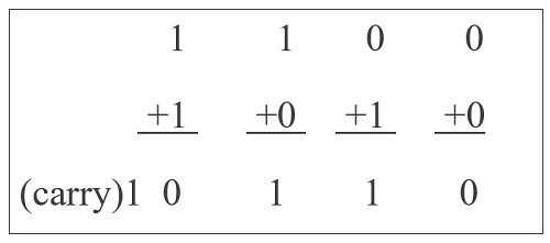
Binary addition is similar to that of decimal addition. Add the first digits of a number and if the count exceeds binary 2, then carry ‘1’ to the next row. Some basic binary additions are shown below.
The adder that performs simple binary addition must have two inputs (augend and addend) and two outputs (sum and carry). The device which performs above task is called a Half Adder. A Full Adder is another circuit which can add three numbers (two bits from the numbers and one carry bit from previous sum).
Half Adder Circuit
Half adder is a combinational circuit that performs simple addition of two single bit binary numbers and produces a 2-bit number. The LSB of the result is the Sum (usually represented as Sum or S0 or ∑0) and the MSB is the Carry (usually represented as COUT).
The block diagram of a half adder is shown below.
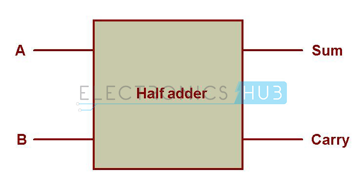
Here, ‘A’ and ‘B’ represents the input two bits that must be added and outputs are ‘Sum’ and ‘Carry’.
Half Adder Truth Table
If we assume A and B as the two bits whose addition is to be performed, a truth table for half adder with A, B as inputs and Sum, Carry as outputs can be tabulated as follows.
| INPUT | OUTPUT | ||
| A | B | Sum | Carry |
| 0 | 0 | 0 | 0 |
| 0 | 1 | 1 | 0 |
| 1 | 0 | 1 | 0 |
| 1 | 1 | 0 | 1 |
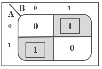
If you observe the truth table, the sum output of the binary addition carried out above is similar to that of an Ex-OR operation, while the carry output is similar to that of an AND operation. The same can be verified with help of Karnaugh Map.
The truth table and K-Map representation for Sum output is shown below.
| A | B | Sum |
| 0 | 0 | 0 |
| 0 | 1 | 1 |
| 1 | 0 | 1 |
| 1 | 1 | 0 |
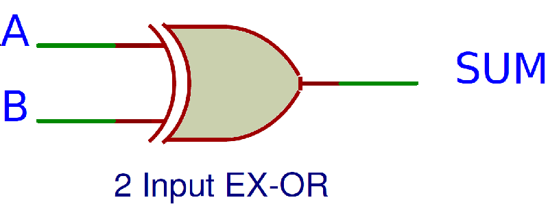
We can derive the Boolean Expression of Sum as follows:
Sum = A B + A B
Sum = A ⊕ B
Hence, the logic diagram for sum is shown below.
The truth table and K Map simplification for carry is shown below.
| A | B | Carry |
| 0 | 0 | 0 |
| 0 | 1 | 0 |
| 1 | 0 | 0 |
| 1 | 1 | 1 |
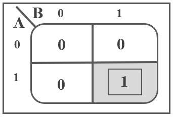
We can derive the Boolean Expression of Carry as follows:
Carry = A B
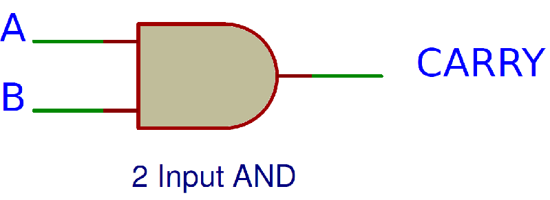
The logic diagram for carry is shown below.
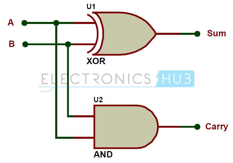
If A and B are binary inputs to the half adder, then the logic function to calculate sum S is Ex – OR of A and B and logic function to calculate carry C is AND of A and B. Combining these two, the logical circuit to implement the combinational circuit of Half Adder is shown below.
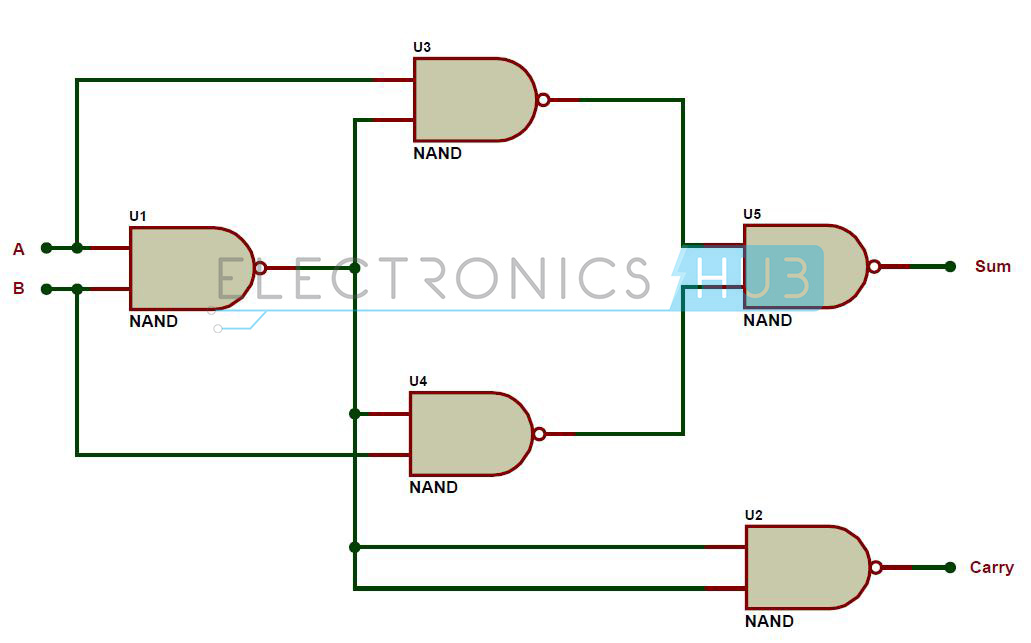
As we know that NAND and NOR are called universal gates as any logic system can be implemented using these two. The Half Adder Circuit can also be implemented using them. We know that a half adder circuit has one Ex – OR gate and one AND gate.
Half Adder using NAND Gates
Five NAND gates are required in order to design a half adder. The circuit to realize half adder using NAND gates is shown below.
Also get an idea about How to Build OR, AND, NOT Gates using NAND Gate
Half Adder using NOR Gates
Five NOR gates are required in order to design a half adder. The circuit to realize half adder using NOR gates is shown below
Limitations of Half Adder
The reason these simple binary adders are called Half Adders is that there is no scope for them to add the carry bit from previous bit. This is a major limitation of half adders when used as binary adders especially in real time scenarios which involves addition of multiple bits. To overcome this limitation, full adders are developed.
Full Adder Circuit
A Full Adder is a Combinational Logic Circuit which performs binary addition on two-digit numbers. Full adders are complex and difficult to implement when compared to half adders.
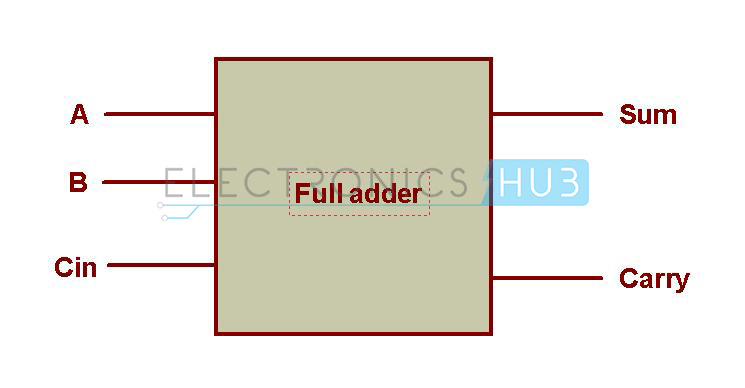
Full adder is a digital circuit used to calculate the sum of three binary bits, which is the main difference between this and half adder. Two of the three bits are same as before which are A, the augend bit and B, the addend bit. The additional third bit is carry bit from the previous stage and is called Carry–in, generally represented by CIN. It calculates the sum of three bits along including the carry. The output carry is called Carry–out and is represented by COUT.
The block diagram of a full adder with A, B and CIN as inputs and S, COUT as outputs is shown below
Full Adder Truth Table
The truth table for full adder is shown below.
| INPUT | OUTPUT | |||
| A | B | CIN | Sum | COUT |
| 0 | 0 | 0 | 0 | 0 |
| 0 | 0 | 1 | 1 | 0 |
| 0 | 1 | 0 | 1 | 0 |
| 0 | 1 | 1 | 0 | 1 |
| 1 | 0 | 0 | 1 | 0 |
| 1 | 0 | 1 | 0 | 1 |
| 1 | 1 | 0 | 0 | 1 |
| 1 | 1 | 1 | 1 | 1 |
Based on the truth table, the Boolean functions for Sum (S) and Carry–out (COUT) can be derived using K–Map.
The K-Map for Sum output (S) of a Full Adder is shown below:
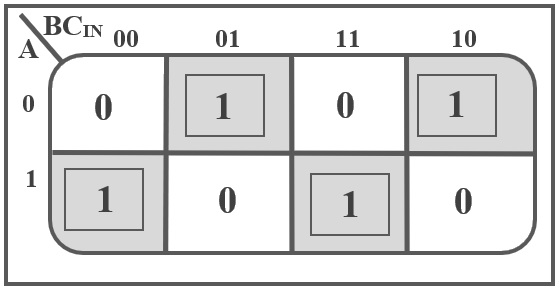
Using the truth table and the above K-Map, the Boolean Expression of Sum (S) output of a Full Adder can be derived as:
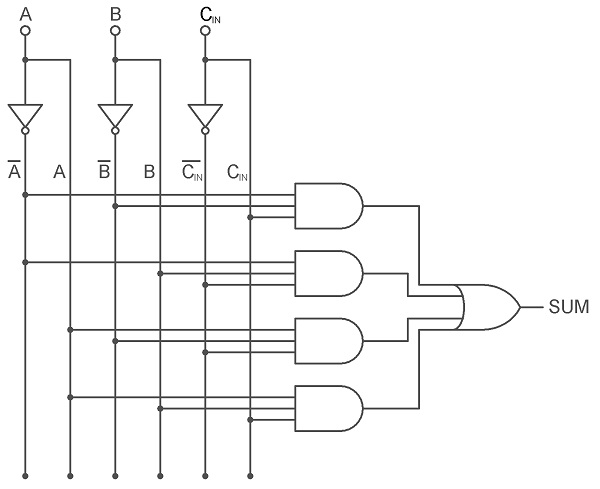
S = A B CIN + A B CIN + A B CIN + A B CIN
From the above Boolean Expression, we can say that the Sum Output of a Full Adder can be implemented using four 3-Input AND Gates, three NOT Gates and one 4-Input OR Gate. The following image shows the logic diagram of the Sum output (S) of a Full Adder.
The K-Map for Carry output (COUT) of a Full Adder is shown below:
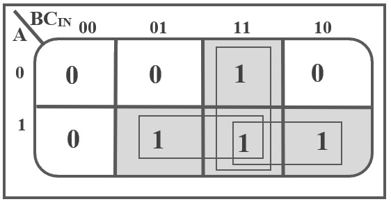
The simplified Boolean equation for COUT is:
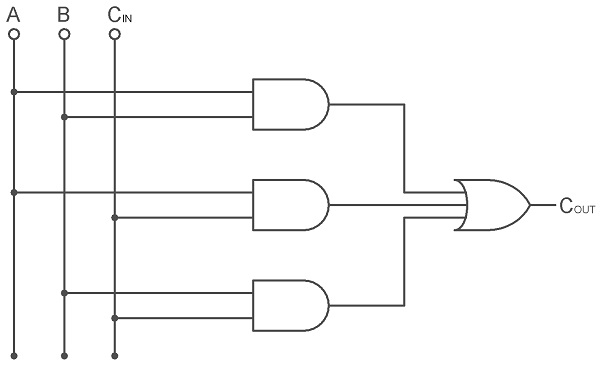
COUT = A B + A CIN + B CIN
From the above Boolean Expression, we can say that the Carry Output of a Full Adder can be implemented using three 2-Input AND Gates and one 3-Input OR Gate. The following image shows the logic diagram of the Carry output (COUT) of a Full Adder.
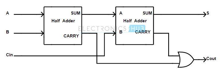
Implementation of Full Adder using Half Adders
A full adder can be formed by logically connecting two half adders. The following is a block diagram that shows the implementation of a full adder using two half adders.
We know the equations for S and COUT of a Full Adder from earlier calculations as:
S = A B CIN + A B CIN + A B CIN + A B CIN
COUT = A B + A CIN + B CIN
We can rewrite the equation for Sum as follows:
S = A B CIN + A B CIN + A B CIN + A B CIN
= CIN (A B + A B) + CIN (A B + A B)
=CIN (A Ex-NOR B) + CIN (A Ex-OR B)
= CIN (A ⊕ B) + CIN (A ⊕ B)
Therefore, S = CIN ⊕ (A ⊕ B)
Similarly, we can rewrite COUT as follows:
COUT = A B + A CIN + B CIN
= A B + A CIN + B CIN (A + A)
= A B + A CIN + A B CIN + A B CIN
= A B (1 + CIN)+ A CIN + A B CIN
= A B + A CIN + A B CIN
= A B + A CIN (B + B) + A B CIN
= A B + A B CIN + A B CIN + A B CIN
= A B (1 + CIN )+ CIN (A B + A B)
= A B + CIN (A B + A B)
= A B + CIN (A Ex-OR B)
Therefore, COUT = A B + CIN (A ⊕ B)
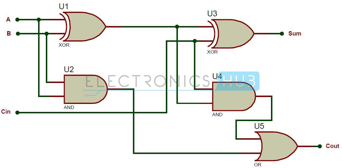
Based on the above two equations, the full adder circuit can be implemented using two half adders and an OR gate. The implementation of full adder using two half adders is show below.
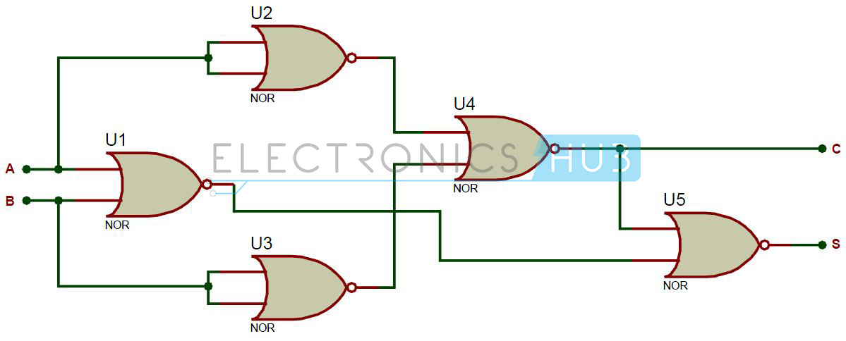
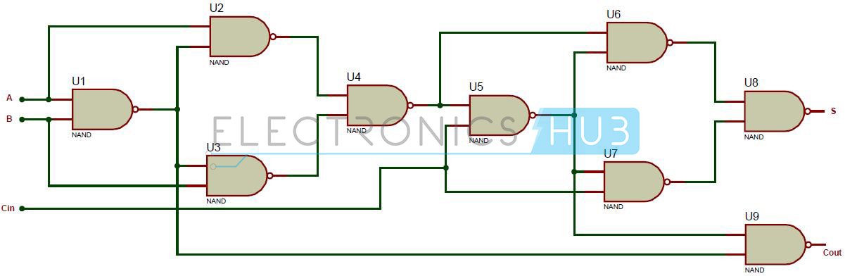
Full Adder using NAND Gates
As mentioned earlier, a NAND gate is one of the universal gates and can be used to implement any logic design. The circuit of full adder using only NAND gates is shown below.
Full adder is a simple 1–bit adder. If we want to perform n–bit addition, then we need ‘n’ number of 1–bit full adders should be used in the form of a cascade connection.
Conclusion
A complete tutorial on Half Adder and Full Adder Circuits. You learned how to implement a Half Adder Circuit, its Boolean Equations, Logic Circuit and also design of Half Adder using NAND and NOR gates, Full Adder Circuit, its Boolean expressions, logic circuit, and implementation of Full Adder using Half Adder.

12 Responses
Impressive . I am putting link of this page to my description section of the adder videos.
Explained very Nicely! A must read. It was worthy reading this section!
Thanks!!
Nice explanation.
Can you please check the expression for the Sum out (S) of the Full Adder? Thanks!
S = A ̅ B ̅ Cin + A ̅ BC ̅ in + ABCin equation is not correct ,
S=S = A ̅ B ̅ Cin + A ̅ BC ̅ in + ABCin +AB ̅ C ̅ in is correct only then , we will get
S= Cin (A ̅ B ̅ + AB) + C ̅ in (A ̅ B + A B ̅ )
we use 01 11 10 in other method we use A bar B And B bar A and AB AB bar so its easy to define and easy to understand
yes. Sum is not correct
THANK YOU, IT HELPED ME TO COMPLETE MY ASSIGNMENT.
Plzzz give me diagr am for 2s compliment by using nand gate ….for project
It gives vrey help in my study
Thankss
Nice! It is helpful for me…..
Thanks alot. Your explanations on this page gave me a perfect understanding.
Nice ? explanation
But derive full adder expression clearly