There are mainly three types of logic gate named AND, OR and NOT gate. And every gate does its own different logic function. So with the help of these basic logic gates, we can get any logical functions or any Boolean or else any logical expression.
Related Post: Design of Basic Logic Gates using NOR Gate
Truth Tables of Basic Logic Gates:
It is important to know the functioning of the each individual gate so to get familiar with the conversion.
1.NOT Gate:
This logical gate is the most simple type of the digital logical circuit. This gate has only two terminals – one is for the input purpose and another is for the output purpose. The input of the gate is a binary number i.e. it can be only one or zero. The output that get at the output terminal of the logic gate is always opposite of the input terminal which means if we give 1 at the input then the output will be 0 and viceversa.
The number of stage that can be possible will be calculated by 2ª (the number of input is calculated by the help of “a”).
Truth Table of NOT Gate is shown below –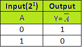
2.AND Gate:
This logic gate consists of two input terminal and one output terminal. The working of these gate is such that at output terminal we will get binary 1 if and only if both the input are binary 1. In the case if any of the input has binary zero then the output we got will be binary 0.
Number of phase possible = 2n =22 = 4.
Truth table of AND gate is shown below –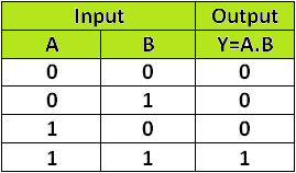
3.OR Gate:
Likewise AND gate, OR gate is one of the other fundamental logic gate which has two input terminal and one output terminal. If any of the input is at the low stage i.e. at binary 0 then the output got will be high i.e. binary 1. In case of only both the input is at binary low stage output will be binary low.
Number of phases can be possible = 2n =22 = 4.
OR gate truth table is shown below – 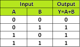
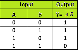
4. NAND Gate:
The NAND gate is just a combination of the expression NOT gate as well as AND gate. Hence the NAND gate is made up of AND gate which is followed by an inverter. The working of these gate is like that we get binary 1 at the output of the gate if and only is both the input is at the binary low state i.e. at 0.While if any of the input terminal is at the binary high i.e. at 1 then the output we got will be binary low state i.e. at 0.
Expression as well as truth table of the NAND gate is shown below –
Transformation of NAND Gate into Other Basic Gates:
1. Construction of NOT Gate with NAND Gate:
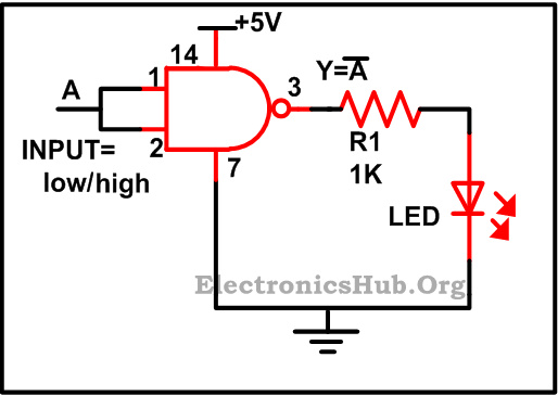
We have need of only one input terminal so both the input terminal of the NAND gate is been shorted by us which you can also find out in the figure above. Now when we give binary 1 at the input terminal we will get 0 at the output due to property of the NAND gate which can be seen from the truth table of the NAND gate.IC7400 is been used by us which is a Quad two terminal input NAND gate.
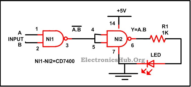
2.Construction of AND Gate with NAND Gate:
3.Construction of OR Gate with NAND Gate:
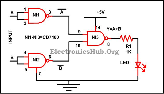
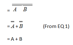
One should be familiar with the DE Morgan’s theorem before getting familiar with these one- It says that the complement of a product is equal to the sum of the complements.
(AB)‾ = A‾ + B‾ —- EQ 1
Through the figure that shown above, Two NAND gates are used, and the input terminal of each gate is been short, so the output we get as = A‾B‾
This output is now given to another NAND gate and the output that we receive here is –
Required Components:
- IC
- CD7402 – 1
- R1 (1K) – 1
- LED – 1

4 Responses
It is good
Very much Helpful. Thank you 🙂
Thanks explain about logic gate.
thank u