In this tutorial, we will learn about one of the major applications of Capacitors as Bypass Capacitor or Decoupling Capacitor.
We know that a Capacitor is an electrical device that is capable of storing energy in the form of electric field and releasing it at a predetermined time and rate. Also, Capacitors block direct current and pass alternating current.
Both these features (or functionalities) of the Capacitor are used in a Bypass Capacitor.
Introduction
Imagine you have designed a nice Op-Amp circuit and started prototyping it and disappointed to find that the circuit doesn’t work as expected or doesn’t work at all. The main reason for this may be Noise from power supply or internal IC Circuitry or even from neighbouring ICs may have coupled into the circuit.
The noise from the power supply due to regular spikes is undesirable and must be eliminated at any cost. Bypass Capacitors act as the first line of defence against unwanted noise on power supply.
What is a Bypass Capacitor?
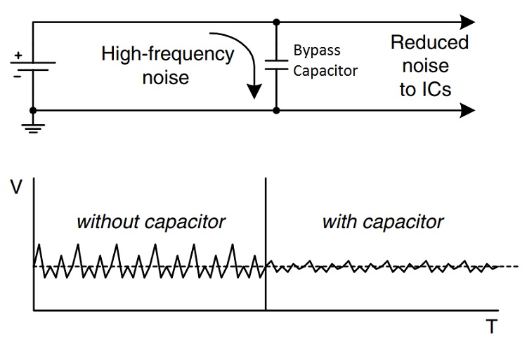
A Bypass Capacitor is usually applied between the VCC and GND pins of an integrated circuit. The Bypass Capacitor eliminates the effect of voltage spikes on the power supply and also reduce the power supply noise.
The name Bypass Capacitor is used as it bypasses the high frequency components of power supply. It is also called as a Decoupling Capacitor as it decouples one part of the circuit from other (usually, the noise from power supply or other ICs is shunted and its effect is reduced on the other part of the circuit).
Bypass Capacitors are generally applied at two locations on a circuit: one at the power supply and other at every active device (analog or digital IC).
The bypass capacitor placed near the power supply eliminate voltage drops in power supply by storing charge and releasing them whenever necessary (usually, when a spike occurs).
Coming to the bypass capacitor placed near VCC and GND pins of an IC will be able to instantaneous current demands of a switching circuit (digital ICs) as the parasitic resistance and inductance delay the instantaneous current delivery.
How Bypass Capacitor Eliminates Power Supply Noise?
To understand how a bypass capacitor eliminates noise, you need to first understand how a capacitor works in DC and in AC. When a capacitor is connected across a DC power supply, like a battery from example, an electric field is developed across the dielectric with a positive charge on one of the conductors and negative charge on the other.
As the capacitor charges, a transient current flows from the supply. But as the charge on the capacitor reaches its maximum (determined by Q = CV), the electric field between the conducting plates of the capacitor nullifies the electric field of the power supply and no more charges flow through capacitor.
Hence, in a DC Circuit, the capacitor charges to the supply voltage and blocks the flow of any current through it.
When a capacitor is connected across a time varying AC power supply, the current flows with little or no resistance due to charging and discharging cycles.
Keeping this in mind, when a Bypass Capacitor is placed across the power supply, it provides a low resistance path for the noise (which is essentially an alternating signal) from supply to ground. Hence, the bypass capacitor shunts the power supply with the nose signals.
Since DC is blocked by the capacitor, it will pass through the circuits instead of passing through the capacitor to ground. This is the reason; this capacitor is also known as Decoupling Capacitor.
Bypass Capacitor Considerations
A circuit without Bypass Capacitor or improper Bypassing can create severe power disturbances and may lead to circuit failure. Hence, an appropriate Bypass Capacitor must be used in the circuit.
The following are a few considerations that must be taken into account when selecting a Bypass Capacitor.
- Capacitor Type
- Capacitor Placement
- Capacitor Size
- Output Load Effect
Capacitor Type
In high frequency circuits, the lead inductance of the bypass capacitor is an important factor. When switching at high frequencies like > 100MHz, a high frequency noise is generated on the power rails and these harmonics in power supply in combination with high lead inductances will cause the capacitor to act as an open circuit.
This prevents the capacitor to supply the necessary current when needed in order to maintain a stable supply. Hence, when selecting a capacitor for bypassing power supply from internal noise of the device (integrated circuit), a capacitor with low lead inductance must be selected.
MLCC or Multilayer Ceramic Chip Capacitors are the preferred choice for bypassing power supply.
Capacitor Placement
The placement of a Bypass Capacitor is very simple. Generally, a Bypass Capacitor is placed as close as possible to the power pin of the device. If the distance increases, the extra tack on the PCB can translate into a series inductor and a series resistor, which lowers the useful bandwidth of the capacitor.
Hence, longer PCB traces between the power pin and the bypass capacitor increases inductance and defeats the purpose of introducing the bypass capacitor in the first place.
Capacitor Size
The size of a bypass capacitor is crucial in determining the ability of the capacitor to supply instantaneous current to the device when needed. There are two things to be considered when determining the size of a capacitor.
- The amount of current required when switching a pin from low to high
- Maximum Pulse Slew Rate to calculate the maximum current of a capacitor
Output Load Effect
If the output load is purely resistive, then the frequency doesn’t affect the rising and falling times of the output. However, if the output load is capacitive, an increase in frequency will cause higher transient current and oscillations in the supply.
Role of Bypass Capacitor in Amplifiers
The following image shows the circuit diagram of a voltage divider biased Amplifier. Resistors R1, R2, RC and RE help the transistor to bias with Q point approximately at the middle of the load line. The resistor RE adds stability to the Q point.
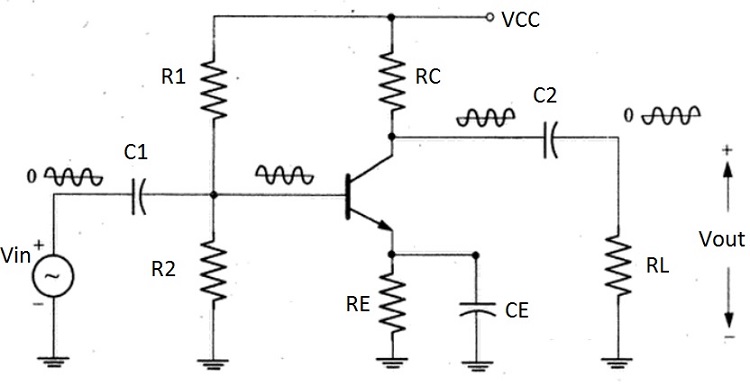
There are two coupling capacitors C1 and C2 at input and output respectively. C1 couples the alternating signal source to the base of the transistor while C2 couples the amplifies signal to the load.
But the device of discussion is the Bypass Capacitor CE. The magnitude of the emitter current is large due to amplification of the ac signal. If there is no bypass capacitor, the large ac emitter current flows through the emitter resistor RE with a large ac voltage drop across RE.
This results in a small ac base current as the voltage drop across the RE subtracts from Vin. Hence, the output voltage decreases and the voltage gain reduces drastically.
We need to provide a low impedance path for the ac emitter current to flow from emitter to ground to prevent a loss of voltage gain. This can be achieved by connecting a capacitor between emitter and ground and this acts as a Bypass Capacitor for bypassing ac emitter current.
Where Bypass Capacitors are used?
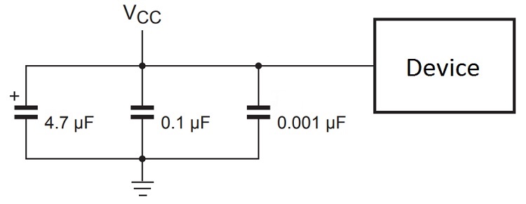
Almost all analog and digital devices use bypass capacitors. In both these devices, a bypass capacitor, usually a capacitor or value 0.1µF, is placed very closely to the power pins. Power supply sources also use bypass capacitors and they are usually the larger 10µF capacitors.
The value of bypass capacitor is dependent on the device i.e. in case of power supplies it is between 10µF to 100µF and in case of ICs, it is usually 0.1µF or determined by the frequency of operation.
If the bandwidth of the device is approximately 1MHz, a 1µF bypass capacitor is used. If the bandwidth is approximately 10MHz or above, a 0.1µF capacitor is used.
In some applications, a network of bypass capacitors in parallel is used to filter a wide range of frequencies.
Every active device in a circuit must have a bypass capacitor placed close to the power supply pin. In case there are multiple bypass capacitors, the smaller capacity capacitor must be placed close to the device.
In analog circuits, a bypass capacitor generally redirects the high frequency components on the power supply to ground. Otherwise, these signals would enter into the sensitive analog IC through the power supply pin. If a bypass capacitor is not used in an analog circuit, there is a good chance that noise is introduced into the signal path.
The use of bypass capacitors in Digital circuits with microprocessor and controllers is slightly different. The major function of bypass capacitors in digital circuits is to act as charge reservoirs.
In digital circuits, where the logic gates are switched at high frequency, there is requirement for a large current during the switching. The parasitic resistance and inductance will not allow sudden flow of huge current that is required in the switching process.
Hence, a Bypass, which is placed as close to the power pin as possible to reduce parasitic inductance, will provide the instantaneous current before the power supply could kick-in.
Applications of Bypass Capacitors
The main purpose of a bypass capacitor is to shunt the undesirable high frequency components of a power supply while passing the desirable DC. The following are the three main areas of application of Bypass Capacitors.
Compensate Current Demands
Bypass capacitors are used to provide the necessary current when demanded. For example, the drive current to a loudspeaker from an amplifier varies according to the signal and the current demands of the amplifier’s output are dependent on the loudness of the signal.
Such varying current at the output causes a varying current drawn from the supply. These variations in the power can cause fluctuations that may be coupled to the signal line as noise through the power supply.
Bypass Capacitors can be helpful in reducing the fluctuations by acting as temporary current sources.
Power Supply Filters
In power supplies, large bypass capacitors usually 100µF or 1000µF or more, are used to filter the ripples of the rectified sine wave.
Digital Systems
In digital circuits, a bypass capacitor is used between VCC and GND pins of all the IC. This helps in maintaining a stable power supply within the recommended range of the IC and also to eliminate high frequency signals from entering the power supply. Additionally, they also act as instantaneous current providers in fast switching circuits.
