A normal P-N junction diode is usually fabricated by adjusting the P-type and N-type semiconductors on a single semiconductor crystal. The characteristics of a junction diode demonstrate that it is designed largely for operating in the forward direction. Applying a large amount of forward bias causes greater forward current with a small value of forward voltage.
However, reverse biasing the diode do not cause conduction of current till high values of reverse voltage are reached. If the reverse voltage is large enough, breakdown occurs and a reverse current starts to flow. Ordinary Junction diodes are generally damaged when this breakdown occurs. The flow of current in zener diodes is controlled by the minority charge carriers under the reverse bias condition, so they can also be referred to as break down diodes.
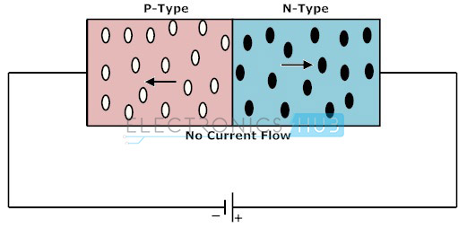
During specific conditions of fabrication, a special type of diode is formed that will not be ruined when the breakdown voltage is increased, given that the current does not exceed a defined limit to prevent the case of overheating. This type of devices is referred to as zener diodes.
Zener Diode Tutorial
Zener diodes are named after Clarence Melvin Zener by the Bell Laboratories, who discovered this type of electrical property. These diodes are a unique kind of diodes with heavy doping concentration at the time of fabrication. Due to the heavy doping, a large number of free electrons and electron holes are created and are responsible for conducting current due to minority carriers in reverse bias.
These diodes are designed to have avalanche characteristic that is very steep. Zener diodes are heavily doped silicon diodes, unlike normal diodes that exhibit an impulsive reverse break-down at comparatively low voltages.
Zener diodes allow current to flow in the forward direction in the similar manner as an ideal diode, and also it permits current to flow in the reverse direction when the voltage is above a certain value known as the breakdown voltage. This voltage can also be referred as zener knee voltage or zener voltage.
If the voltage across the diode is increased, temperature increases and crystal ions vibrate with greater amplitude and all these leads to the breakdown of the depletion layer. When breakdown occurs, there will be a sharp increase in reverse current. A large amount of varying reverse current can pass through the diode without damaging it.
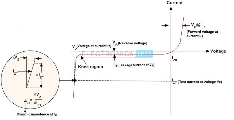
So zener diodes are intended to function in the reverse breakdown region with a reverse breakdown voltage (Vz) in the range 2.4 V to 200 V. The value of Vz depends on the doping concentration. When the Zener voltage is reached, the zener diode conducts current from its cathode terminal to its anode terminal.
The breakdown voltage or zener voltage across the zener diode fairly remains constant. The maximum amount of reverse current is limited by the wattage rating of the diode.
There are many different kinds of Zener diodes. They categorized by power dissipation, nominal working voltage, forward current, forward voltage, packaging type and maximum reverse current. General values for working zener knee voltage are 5.1 V, 6.2 V, 15 V and so on. Forward current can have a range from 200uA to 200A with the most common forward current being 10mA or 200mA.
Zener diodes found its use in several applications. They are widely used as voltage reference diodes in electronics circuits that allow simple and stable reference voltage regulator circuits to be prepared, as well as they are cheap and easy to manufacture.
They can be used as surge suppressors for device protection, in clipping circuits for clipping the waveforms that are not required, in different switching operations, as reference elements and they can be used to remove spikes that may damage a circuit or cause it to overload.
The unvarying reverse voltage of a zener diode renders it as a very useful component in controlling the output voltage against the variations in load resistance or variations in the input voltage provided from an unstable voltage source such as the battery bank of a renewable energy system which will fluctuate depending on the state of charge of the bank. The current through the Zener diode will change to keep the voltage within the adjustable threshold limits of zener action.
Manufacturers rate zener diodes according to their Vz value and the maximum power dissipation at room temperature i.e., 25ºC. This is an indication of the maximum reverse current that a zener diode can safely conduct electric current. Each zener knee voltage value is generally specified at lowest zener current. As a result the power dissipation values are used to indicate the safe operating range. Typical values of power dissipation ratings are from 150mW to 50W.
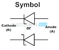
Zener diode can be identified by the terminal that is by observing a black color ring at cathode terminal. If the diode is an SMD component, then a colour band will be available for cathode terminal. By recognizing the zener diode code marked over the device, we can determine the value of it.
Zener Diode I-V Characteristics Curve
In the forward bias condition, the zener diode behaves like an ideal diode within specified current and power limits, but it differs in reverse bias condition where the zener diode has very steep avalanche characteristic at the breakdown voltage in reverse bias condition.
Zener operates mainly in the reverse bias mode by connecting anode to the negative terminal of the power supply. Zener diodes are categorised and rated by the voltage at which they will turn on or start to conduct the reverse bias current.
The maximum power intended for a zener diode is specified as Pz=VzIz max and it is a function of the plan and structure of the diode. The knee of the curve is generally approximated as 10% of Iz max, i.e., Iz min=0.1Iz max.
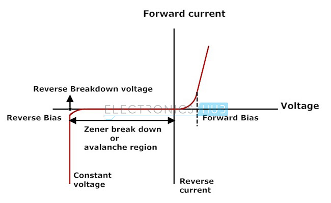
Generally these zener diodes are used to regulate the voltage. In reverse bias condition after the break down zener diode provides a constant output voltage even if we increase the input voltage. There are specifically two separate mechanisms that might cause a breakdown in a zener diode:
Avalanche Breakdown
It is predominant above approximately 5.5 volts. This mechanism is also referred to as impact ionisation or avalanche multiplication. For reverse conduction it is necessary to visualise the phenomenon of avalanche breakdown. This process begins when a large negative bias is applied to the PN junction, sufficient energy is imparted to thermally generated minority charge carriers in the semiconductors.
As a result the free carriers acquire required kinetic energy to break the covalent bonds and create an electric field through collisions with crystal particles. The charge carriers created in collision contribute to the reverse current, well beyond the normal reverse saturation current and may also possess enough energy to participate through collisions, creating an additional electric field and the avalanche effect by impact ionization, once a sufficiently high reverse bias is provided this process of conduction takes place very much like an avalanche: a single electron can ionise several others.
Zener Breakdown
It is predominant below approximately 5.5 volts. This mechanism is also referred to as a high field emission mechanism. The phenomenon of zener breakdown is related to the concept of avalanche breakdown. Zener breakdown is achieved by heavily doped regions in the neighbourhood of ohmic contact.
It is the second method of disturbing the covalent bonds of the crystal atoms and increasing the reverse bias zener diode current, to be sustained at a much lower specific voltage than normal diode. The reverse bias voltage known as zener voltage, where this mechanism occurs is determined by the diode doping concentration and it occurs when the depletion layer field width is sufficiently enough to disrupting the covalent bonds and cause number of free charge carriers due to electric field generation to swell.
The true Zener effect in semiconductors can be explained in terms of two upper energy bands are of interest. The two upper energy bands are namely the conduction band and the valence band.
Either of these effects or a combination of the two mechanisms significantly increases the current in the reverse bias region while having a negligible effect in the voltage drop across the junction. When the applied reverse bias voltage is greater than a predetermined voltage, zener breakdown takes place.
The zener breakdown voltage is made sharp and distinct by controlling the doping concentration and when surface imperfections are avoided. The voltage across the zener diode in breakdown region is almost constant that turns out to be an essential concept in regulating the voltage.
Zener Diode as Voltage Regulator
I-V characteristics of zener diode make it suitable for application such as a voltage regulator. A voltage stabilizer is a combination of elements that are designed to ensure the output voltage of a supply fairly remains constant. Excess voltage protection is done by using zener diodes because there will be reverse current due to minority charge carriers starts flowing through the diode after the reverse bias voltage exceeds a certain value.
Keeping the zener diode in parallel with a variable load resistance RL, ensures a constant output voltage even though the load current and the supply voltage varies. In practical circuits the simplest form of current source is a resistor. The key in using the zener diode as voltage regulator is that as long as the zener diode is reverse biased, the flow of current greater than a few micro amperes must be accompanied by a voltage greater than the Zener voltage.
This type of arrangement of the circuit provides safety for equipment connected to terminals. This arrangement of regulator circuit is referred to as a shunt regulator in which the regulating element is placed in parallel with the load. The input voltage to the system is a few volts and as long as it is more than the desired output voltage, a stable voltage will be produced across the zener diode.
Usually the reverse current should not exceed normal value but, if due to any fault in circuit construction the current exceeds maximum allowable limit, the system will damage permanently. However to avoid unbalanced performance, zener diodes are used for voltage reference in many measuring instruments.
As the input voltage increases, current through the zener diode increases, but the drop in voltage remains constant which is the necessary feature required for zener diodes. Therefore, reverse current in the circuit has increased, voltage drop across the resistor increases by an amount equal to the difference between the applied input voltage and the zener knee voltage of the zener diode.
The output voltage of regulator system is fixed as the zener knee voltage of the zener diode and can be used in power devices requiring a fixed voltage of firm value. The zener diode will continue in regulating the voltage till the zener diode current falls below the minimum Iz min value in the reverse breakdown region.
Zener Diode Regulator
At the time of initiation, choose the zener diode based on the voltage required. Construction of a voltage regulator is easy with the help of an ideal Zener diode, merely connecting the diode between the unregulated source of voltage and ground.
The source resistance Rs is connected in series with zener diode to limit the flow of current through the diode with voltage source connected across the combination. The cathode terminal of zener diode is connected to the positive terminal of the voltage source so that the zener diode is biased in reverse condition and will be operating in breakdown region.
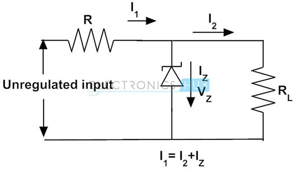
When the load is not connected across the zener diode, no load current will be conducted and all the current due to the circuit will pass through the zener diode dissipating maximum amount of power that causes overheating of the diode and damages permanently.
Selecting the appropriate values of series resistance Rs is also important because it also causes greater diode current, so that maximum power dissipation of the diode should not be exceeded under no load or at high impedance condition.
Whenever a load is connected in parallel with zener diode, voltage across the load is same as the zener diode voltage. However the source voltage must be greater than the zener voltage and the upper limit of zener current depends on the power rating of the zener diode; otherwise the zener voltage will simply follow the applied input voltage.
It is also necessary that both zener diode and resistor should have a high rating of power to handle all of the current across the circuit. If a decoupling capacitor is present across the zener diode, it is more useful in providing additional smoothing to the DC supply which is necessary to stabilize the voltage.
Zener Diodes in Series
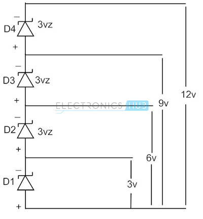
When two or more than two zener diodes are in a manner such that the cathode of the first zener diode is connected to the anode of the second zener diode similarly cathode of the second zener diode is connected to the anode of the third zener diode, such a type of connection is referred to as a series connection of zener diodes. In this connection the total voltage across the circuit is equal to the sum of the voltages of all zener diodes in the connection.
From the figure shown above, 3V zener diodes are connected in series. The total zener voltage of this series connection is 9V. The zener voltage ratings of the individual zener diodes should be best chosen for most of the applications.
A characteristic zener diode for general purpose electronic circuits has the power rating of 500mW, BZX55 zener diode series or the larger 1.3W, BZX85 zener series are most commonly used zener diodes. The 500mW, BZX55 series zener diodes are generally available in the range varying from 2.4 Volts to nearly about 100 Volts.
Zener Diode Voltages
BZX55-Series:
Power Dissipation: 0.5 W
BZX85-Series:
Power Dissipation: 1.3 W
Zener Diode Clippers
Zener diode based clipping circuits limit the certain part of the input waveform that is applied across the input terminals, these zener diode clippers are generally used for protecting the circuits and in shaping of the input waveforms. Consider a clipper circuit as shown in the figure. If we want to clip the waveform above 3.2 V, we will use a 3.2 V zener diode.
The output waveform can be clipped on the positive side by greater than 3.2 V and there maintains a constant output. The waveform on the negative side is clipped at 0.7 V and there after the zener diode turns ON and acts as a silicon diode.
The diode and power supply as shown will prevent the output voltage from exceeding 0.7V. Zener diode clipping circuits are used to eliminate noise in amplitude and spikes in voltage, voltage regulation and to make fresh waveforms from an existing signal such as squaring off the peaks of a sinusoidal waveform to obtain a rectangular waveform.
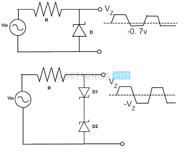
Connecting the zener diodes in opposite direction, back to back fashion produces an AC regulator that can be used as a square wave generator. It is the most commonly used zener diode connection for clipping the waveforms and protecting the electronic circuits from over voltage.
Both the zener diodes are usually connected across the input terminals of the power supply, at some point in the normal functioning, one of the zener diode in the circuit is OFF and the other zener diode have no or very little affect.
On the other hand if the applied input voltage to the circuit exceeds the maximum limit, then the zener diode is turned ON and it will clip the applied input signal for protecting the circuit.
