Logic gates are the basic elements in digital world. In the previous article we have learnt about basic logic gates. These basic gates can be constructed from the universal gates. There are two universal gates in the digital logic. They are NAND gate and NOR gate.
If these gates are fabricated properly other basic gates can be constructed easily. For this reason they are called universal gates.As they are easy to fabricate and economical ,these gates are popularly used.
This article explains about one of the universal gates called NAND gate.
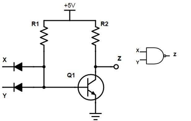
NAND gate Logic Symbol and equivalent circuit
NAND gate is the combination of AND gate and NOT gate. It has the capability to perform the operations of 3 logic gates such as OR, AND gate and NOT gate. The outputs of AND gate and NAND gates are inverse to each other. One should know the fact that AND gate is constructed from the AND gate.
It has 2 inputs X, Y and single output, Z. The equivalent circuit of NAND Gate using diodes and transistors is shown below.
The inputs to the NAND gate is applied through the diodes and these diodes are connected to BJT.
When the inputs of both diodes of NAND gate are connected to a high voltage level i.e. +5 V (logic HIGH), then the 2 diodes will be reverse biased. Since the diodes don’t conduct, they both will be in OFF state. At this condition , transistor Q1 is capable for driving the supply voltage from the resistor.
This makes the transistor to be in ON state, so the voltage at the output Vce (Sat) will be 0. In the same way, if we apply the low voltage supply to both the diodes (logic low) i.e. 0, then no current flows through the transistor, so it will become OFF. This makes the output to become HIGH.
The circuit and logic symbol for NAND gate is given below.
Mathematical expression for NAND gate operation is given as Z =(X.Y) ̅. Where, bar “ ̅“represents the reverse operation.
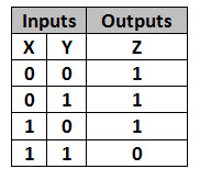
Nand Gate Truth Table
From the truth table, it can be observed that NAND gate output will be high if any of its input is at low state. It will become HIGH if both the inputs are High.
2 – Input Transistor NAND Gate
NAND gate can be designed by using transistors also.To design a 2 –input transistor NAND gate, we connect two resistors to bases of the two transistors. The supply voltage of +6 V is passed to the collector of first transistor, through a resistor.
The output is collected across the collector of the transistor and the resistor. The 2 transistors are connected in series i.e. the emitter of the first transistor is connected to the collector of the second transistor and the emitter of the second transistor is grounded.
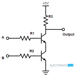
The resistors connected at the input side are of each 10K ohms.
Pulsed Operation
If we apply 2 different clock signals as the inputs of NAND gate X and Y, then the output of the NAND gate is shown below (X, Y are inputs and Z is output)
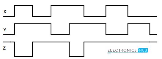
When both inputs are high, then the output of the NAND gate will be LOW and when either of the inputs is low, then the output goes to HIGH level. At the end of the clock pulses in the above, the output is at high level as one of the inputs is low.
Universal NAND gate
NAND gates are called “Universal gates”. This is because , This gate can function as any of the basic logic gates by just making some changes at its input side. Mostly, we prefer NAND gates over NOR gates for designing the other basic logic gates. Let’s see why these are preferred and how we can design other gates by using NAND gate.
Why we prefer NAND gate over NOR, to design basic logic circuits?
The area occupied by NOR gate is more than that of the area occupied by NAND gate. As the occupied area is high, the capacitance associated with the NOR gate is also high. This cause to occur more delay, as the time required for the input to reach output becomes high.
Another reason for opting NAND gate is its low “logic effort”. We can realize a logic gate by 2 methods. The first and most used method is Boolean function method and the second method is logic effort method. The logical effort of a NOR logic gate is 5/3 and for NAND gate it is 4/3.
The gate with low logic effort is the better one to use. So, as the NAND gate has the low logic effort, it is speed and better output is provided when the load at its input is reduced.
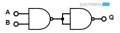
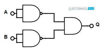
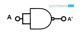
Basic Logic Gates using only NAND Gates
We can design basic logic gates such as AND, OR, NOT gates. Let’s see mow a NAND gate can perform all the 3 types of functioning.
3 -Input NAND gate
Multi input NAND gates can be designed by connecting other logic gates at its input side. Let’s see the logic symbol and truth table of 3 –input NAND gate. There is no change in Boolean expression with change in number of inputs. The output of NAND gate is the inverse of multiplication of NAND inputs.
3-Input NAND gate symbol
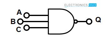
The Boolean expression for the 3-input NAND gate is Q = (A.B.C) ̅
Truth table of 3 – input NAND Gate
The truth table of 3 –input NAND gate is given below
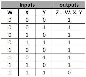
The output of the 3 input NAND gate is LOW when all the 3 inputs are HIGH and it will be HIGH for all other combinations of inputs.
4-Input NAND gate
Similar to 3-input NAND gates, we can also design 4-input NAND gate.
Its Boolean expression is Q = (A.B.C.D) ̅
Odd numbered NAND gate can be designed by making one of the inputs ‘unused’. The function of Logic NAND gate is also known as Shaffer Stroke Function. This is denoted by upward arrow or vertical bar, as A NAND B = A|B or A↑B.
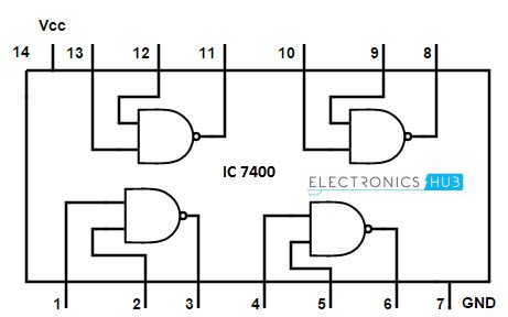
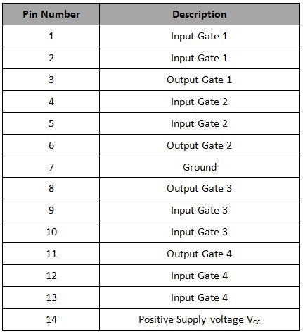
Commonly available TTL and CMOS logic NAND gate IC
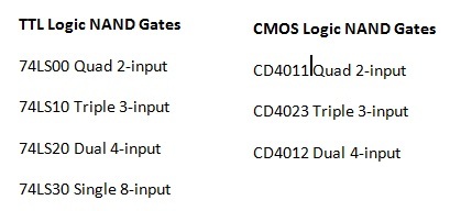
7400 Quad 2-input Logic NAND Gate IC
The specifications of 7400 NAND IC are
- Maximum Supply voltage is 5.25V.
- Minimum Input voltage 2.0.
- Output current is 8mAV.
- Operating temperature is 75° max.
NAND Gate Applications
Logic NAND gate has many applications like Burglar alarm, freezer buzzer etc.
Burglar alarm or theft alarm
The burglar alarm circuit is shown below. It has a NAND gate with an LDR input. LDR means Light Dependent Resistor. When the alarm switch is closed, then one of the NAND gate inputs will be low. And if the LDR is kept in light, then the second input is also low. So the 2 inputs of the NAND gates are low. So if any of the two situations occurs, the output of NAND gate becomes HIGH and then the theft alarm rings, as a sign of alert.
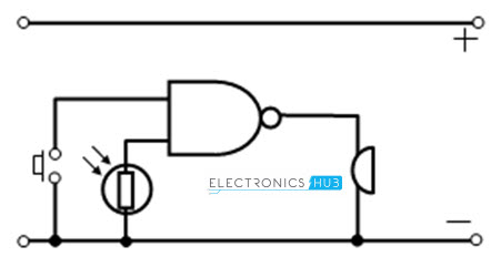
The Burglar alarm is an electronic device which is used to detect the unauthorized entry, and as a security alarms and theft alarms. These are used in commercial as well as residential and military security purposes against intruders. These alarms can be connected to television sets and closed circuit television surveillance systems.
Freezer warning buzzer
This freezer warning buzzer circuit uses NAND gate as a NOT gate. The single input NAND gate (functioning as NOT gate) has two thermistors at its input side. Whenever the thermistor is cold, its resistance will be high so the input of NAND gate will be HIGH. As the NAND gate is functioning as a NOT gate, the output of the NOT gate will be LOW.
Similarly, when the Thermistor gets warmer, its resistance will decrease. So the voltage drop across the Thermistor will be low, making the input of the NAND gate to become LOW.
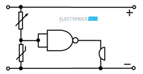
When the voltage drop across the two Thermistors will be low, then the output of the NAND gate will become high and then the Buzzer rings.
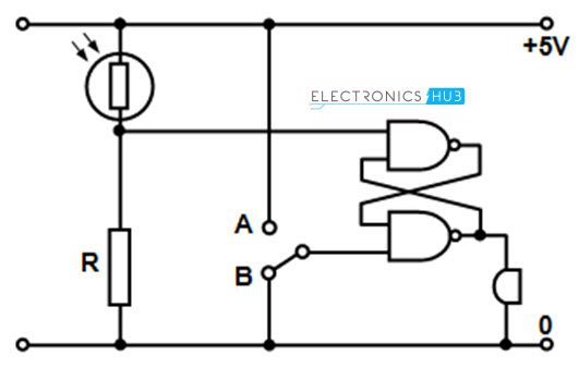
Light activated theft alarm
This circuit consists of NAND gates connected in the form of a simple latch circuit. When the switch is connected to ‘A’, the buzzer inputs will be off. At this condition there is no effect of LDR (which is connected as one of the inputs of Latch) on the circuit. But when the switch is at ‘B’ then the buzzer will be ON due to the effect of LDR. The buzzer will sound simultaneously the light or flash light also flashes up to alert. Buzzer can be turned off only by returning the switch to position ‘A’.
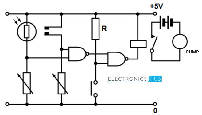
Automatic watering system
This technological invention is useful for water plants at night time. This circuit functions only when the LDR will OFF (generally happens at night time) and when the surrounded atmosphere of the Thermister is wet. This circuit has a relay to act as switch which allows pumping the water only when the two input conditions of the NAND gate are fulfilled.