The simplest way to communicate between a computer and a microcontroller is through UART i.e. Universal Asynchronous Receiver Transmitter. It is a type of Serial Communication Protocol and it uses only two wires for transferring the data. Normally, we need to connect the microcontroller to the computer using a COM Port. But the modern day computers and laptops doesn’t include a COM port as the USB ports have replaced them.
Hence now – a – days, the interface between a microcontroller and the computer is through USB Port with the help of USB – to – RS232 modules that are based on the USB – to – UART Bridge ICs like CP210x from Silicon Labs or FT232R from FTDI.
Basics of UART
Before going to the UART Programming in LPC2148 MCUs, let us first see some basics of the UART Protocol. As mentioned earlier, the UART Protocol uses only two wires (or pins in a device like microcontroller) to transmit the data. In that, one is for transmitting the data and the pin is called TX pin in the device. The other pin is used to receive the data and is called RX pin.
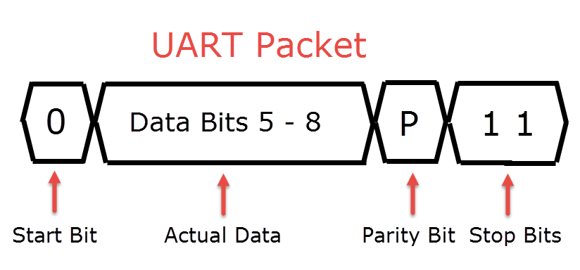
As UART is a serial communication, the data is transmitted in a series of packets. Usually, a packet consists of 4 parts: a start bit, the actual data, a parity bit and stop bits. The following image shows a typical structure of the data packet in UART.
UART in LPC2148
Coming to UART in LPC2148, the LPC214x series of MCUs have two UART blocks called UART0 and UART1. Each UART block is associated with two pins, one for transmission and the other for receiving.
In UART0 block, the TXD0 (Transmit) and RXD0 (Receive) pins in the device are P0.0 and P0.1 respectively. In case of UART1, the TXD1 and RXD1 pins are P0.8 and P0.9 respectively.
| UART0 | UART1 | ||
| TXD0 | P0.0 | TXD1 | P0.8 |
| RXD0 | P0.1 | RXD1 | P0.9 |
Both the UART modules are identical, except the UART1 block has an additional full modem interface. This includes all the pins for RS232 compatibility like flow control pins (CTS, RTS) etc.
Both the UART blocks have 16 byte Receive and Transmit FIFO structures to hold the transmit and receive data. In order to control the data access and assembly, the UART blocks have two registers each.
For the transmitter operation, the TX has two special registers called Transmit Holding Register (THR) and Transmit Shift Register (TSR). In order to transmit the data, it is first sent to THR and then moved to TSR.
For the receiver operation, the RX has two special registers called Receiver Buffer Register (RBR) and Receive Shift Register (RSR). When the data is received, it is first stored in the RSR and then moved to RBR.
Registers associated with UART in LPC2148
There are many registers involved with the UART blocks. UART0 and UART1 have a similar register structure and here we are mentioning some of the important registers of the UART0 block. In order to access the registers in UART1 block, simply replace the ‘0’ with ‘1’.
UART0 Receiver Buffer Register (U0RBR): The Receiver Buffer Register consists of the top byte of the RX FIFO. This is the data that is first arrived and Bit 0 contains the oldest data. In case the received data is less than 8 bits, the remaining bits are padded with 0’s. In order to access the U0RBR register, the Divisor Latch Access bit (DLAB) in the UART0 Line Control Register (U0LCR) must be set to 0. With reference to the user manual, it is advised that the U0LSR register is read first and then the U0RBR register is read.
UART0 Transmit Holding Register (U0THR): The Transmit Holding Register consists of the top byte of the TX FIFO i.e. the oldest data. Bit 0 (LSB) is the first data to be transmitted. In order to access the U0THR register, the Divisor Latch Access Bit (DLAB) bit in the UART0 Line Control Register (U0LCR) must be made zero.
UART0 Divisor Latch Registers (U0DLL and U0DLM): The Divisor Latch Registers determine the baud rate of the UART0. The Divisor Latch is a part of the Baud Rate Generator. The U0DLL and U0DLM registers contains the lower and higher 8 – bits of the divisor and together they form the 16 – bit divisor value. Since it contains the divisor value, the U0DLL cannot contain 0x00 as division by zero is invalid. Hence, the minimum value for the U0DLM:U0DLL combination is 0x00:0x01. In order to access the Divisor Latch Registers, the Divisor Latch Access Bit (DLAB) bit in the UART0 Line Control Register (U0LCR) must be set to 1.
UART0 Fractional Divider Register (U0FDR): The Fractional Divider Register contains the bits that control the prescale for the baud rate generator. U0FDR contains the divisor and multiplier values for prescaling. Both the divisor (DIVADDVAL) and multiplier (MULVAL) values are stored as 4 – bit values. Bit 0 to Bit 3 in U0FDR contains the pre – scaler divisor value for baud rate generation. For the baud rate generator to have an impact on the baud rate of the UART, the divisor value must not be 0. Bit 4 to bit 7 in U0FDR contains the pre – scaler multiplier value. For proper working of the UART0, the value in multiplier must be greater than or equal to 1. This is also applicable even if the baud rate generator is not used.
UART0 Interrupt Enable Register (U0IER): The Interrupt Enable Register is used to enable or disable the interrupts corresponding to UART0. Bit 0 is for RBR Interrupt, Bit 1 is for THRE interrupt, Bit 2 is for RX Line Status Interrupt, Bit 8 is for End of Auto – baud interrupt and Bit 9 is for Auto – baud Time out interrupt. When a bit is 0, the interrupt is disabled and when the bit is 1, the interrupt is enabled.
UART0 Interrupt Identification Register (U0IIR): The Interrupt Identification Register is used to provide the code for priority and status of the pending interrupt.
UART0 FIFO Control Register (U0FCR): The FIFO Control Register controls the operation of the RX and TX FIFOs in UART0. Bit 0 is used to enable or disable the FIFO. Bit 1 is used to reset the RX FIFO. Bit 2 is used to reset the TX FIFO. Bits 6 and 7 are used to control when the interrupt must occur i.e. after how many receiver characters.
UART0 Line Control Register (U0LCR): The Line Control Register is used to set the format of the data which is transmitted or received.
| Bit | Name | Value | Description |
| 1:0 | Word Length | 00 | 5 bit data length |
| 01 | 6 bit data length | ||
| 10 | 7 bit data length | ||
| 11 | 8 bit data length | ||
| 2 | Stop Bit | 0 | 1 stop bit |
| 1 | 2 stop bits | ||
| 3 | Parity Enable | 0 | Disable Parity |
| 1 | Enable Parity | ||
| 5:4 | Parity Select | 00 | Odd Parity |
| 01 | Even Parity | ||
| 10 | Forced 1 parity | ||
| 11 | Forced 0 parity | ||
| 6 | Break Control | 0 | Disable break transmission |
| 1 | Enable break transmission | ||
| 7 | Divisor Latch Access Bit (DLAB) | 0 | Disable access to Divisor Latches |
| 1 | Enable access to Divisor Latches |
UART0 Line Status Register (U0LSR): The Line Status Register gives us the information about the RX and TX blocks in UART0.
| Bit | Symbol | Value | Description |
| 0 | Receiver Data
Ready |
0 | U0RBR is empty |
| 1 | U0RBR contains valid data | ||
| 1 | Overrun Error | 0 | Overrun error status is inactive |
| 1 | Overrun error status is active | ||
| 2 | Parity Error | 0 | Parity error status is inactive |
| 1 | Parity error status is active | ||
| 3 | Framing Error | 0 | Framing error status is inactive |
| 1 | Framing error status is active | ||
| 4 | Break Interrupt | 0 | Break interrupt status is inactive |
| 1 | Break interrupt status is active | ||
| 5 | Transmitter Holding Register Empty | 0 | U0THR contains valid data |
| 1 | U0THR is empty | ||
| 6 | Transmitter Empty | 0 | U0THR and/or the U0TSR contains valid data |
| 1 | U0THR and the U0TSR are empty | ||
| 7 | Error in RX FIFO | 0 | U0RBR contains no UART0 RX errors |
| 1 | At least one UART0 RX error in U0RBR |
UART0 Transmit Enable Register (U0TER): The Transmit Enable Register is used to enable the data transmission i.e. it is used to enable implementation of software flow control. The Bit 7 in U0TER register i.e. TXEN is the only bit available for user. When this bit is high, the UART0 TX will keep on sending data. When this bit becomes 0, the data transmission will stop.
Baud Rate Generation in UART
The formula for calculating UART baud rate is given below
Baud Rate =
The following rules must be followed for the Baud rate generation.
Minimum value for MULVAL must be 1 i.e. 0 < MULVAL <= 15.
The value for DIVADDVAL can be between 0 and 15 with both the extremes included i.e.
0 <= DIVADDVAL <= 15.
In order to get a baud rate of 9600 (which is the most common baud rates) at a peripheral clock frequency of 60 MHz, the following calculations must be followed.
Try with DLM (U0DLM) = 0, DIVADDVAL = 0, MULVAL = 1. By substituting these values in above formula, then we get DLL (U0DLL) as 390.625. Since U0DLL is an 8 – bit register, this value is out of range.
By continuing this trial and error method, we end up at the following settings in order to get a baud rate of 9600 (approximately) with PCLK being 60 MHz.
U0DLM = 1
U0DLL = 110
DIVADDVAL = 1
MULVAL = 15
UART Programming in LPC2148
We will see the configuring and initialization of the UART0 block in the following example where we send some data to the Computer.
#include <lpc214x.h>
#define New_Line 0xA
void UARTWrite(char data);
int main(void)
{
char msg[] = { ‘E’,’l’,’e’,’c’,’t’,’r’,’o’,’n’,’i’,’c’,’s’,’ ‘,’H’,’u’,’b’,’\0′ };
int c=0; // counter
/* Configuring PLL for generation of 60 MHz CCLK and PCLK */
PLL0CON = 0x01;
PLL0CFG = 0x23;
PLL0FEED = 0xaa;
PLL0FEED = 0x55;
while(!(PLL0STAT & 0x00000400));
PLL0CON = 0x03;
PLL0FEED = 0xaa;
PLL0FEED = 0x55;
VPBDIV = 0x01;
/*Configure and Initialize UART */
PINSEL0 = 0x5; /*Select TxD for P0.0 and RxD for P0.1*/
U0LCR = 0x43; /*8 data bits, no Parity, 1 Stop bit | DLAB is set to 1*/
U0DLL = 0x6e; /* DLL set to 110*/
U0DLM = 0x01; /* DLM set to 1*/
U0FDR = 0xf1; /* MULVAL bits – 7:4) is set to 15 and DIVADDVAL (bits – 3:0) is set to 1*/
U0LCR &= 0x0f; // Set DLAB=0 to lock MULVAL and DIVADDVAL
while (1)
{
while( msg[c]!=’\0′ )
{
UARTWrite(msg[c]);
c++;
}
UARTWrite(New_Line);
c=0;
}
}
void UARTWrite(char data)
{
while ( !(U0LSR & 0x02 ) ); // wait till the THR is empty
U0THR = data;
}

2 Responses
Hello Admin! I’ve found two mistakes in this tutorial (https://www.electronicshub.org/lpc2148-uart-tutorial/). They are,
1)U0LCR should not be 0x43 to set DLAB. It has to be 0x83
2)while(!(U0LCR & 0x02)) is actually wrong to check for THR status, it is while(!(U0LCR & 0x20)).
This is just to make you aware of the mistakes, so that no one gets misguided. Thank You!
Hi, Thanks for pointing them out. We will check them and make necessary changes.