The Hartley oscillator is one of the classical LC feedback circuits and used to generate high frequency waveforms or signals. As we discussed in the LC oscillators article that if the reactance elements X1 and X2 are chosen as inductors and X3 as capacitor in the feedback network, then the oscillator is called as Hartley oscillator.
These can be implemented by using different circuit configurations. The major parts of the Hartley oscillators are the amplifier section and the tank section. The tank section consists of two inductors and one capacitor. Each section produces a phase shift of 180 degrees of the AC signal voltage and hence it produces a sine wave voltage.
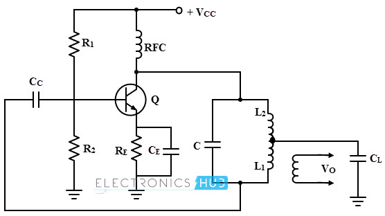
Hartley Oscillator Circuit
The circuit diagram of a Hartley oscillator is shown in figure below. An NPN transistor connected in common emitter configuration serves as active device in amplifier stage. R1 and R2 are biasing resistors and RFC is the radio frequency choke which provides the isolation between AC and DC operation.
At high frequencies, the reactance value of this choke is very high; hence it can be treated as open circuit. The reactance is zero for DC condition hence causes no problem for DC capacitors. CE is the emitter bypass capacitor and RE is also a biasing resistor. Capacitors CC1 and CC2 are the coupling capacitors.

When the DC supply (Vcc) is given to the circuit, collector current starts raising and begins the charging of the capacitor C. Once C is fully charged, it starts discharging through L1 and L2 and again starts charging.
This back-and-fourth voltage waveform is a sine wave which is a small and leads with its negative alteration. It will eventually die out unless it is amplified.
Now the transistor comes into the picture. The sine wave generated by the tank circuit is coupled to the base of the transistor through the capacitor CC1.
Since the transistor is configured as common-emitter, it takes the input from tank circuit and inverts it to a standard sine wave with a leading positive alteration.
Thus the transistor provides amplification as well as inversion to amplify and correct the signal generated by the tank circuit. The mutual inductance between the L1 and L2 provides the feedback of energy from collector-emitter circuit to base-emitter circuit.
The frequency of oscillations of this circuit is
fo = 1/ (2π √ (Leq C))
Where Leq is the total inductance of coils in the tank circuit and is given as
Leq = L1 + L2 + 2M
For a practical circuit, if L1 = L2 = L and the mutual inductance is neglected then the frequency of oscillations can be simplified as
fo = 1/ (2π √ (2 L C))
In some circuits, there exists mutual inductance between L1 and L2 of a transistorized Hartley oscillator as shown in figure below.
Mutual Inductance in Hartley Oscillator
The change in current through coil induces the current in other vicinity coil by the magnetic field is called as mutual inductance. It is an additional amount of inductance caused in one inductor due to the magnetic flux of other inductor.
By considering the effect of mutual inductance, the total inductance of the coils can be calculated by the formula given below.
Leq = L1 + L2 + 2M
Where M is the mutual inductance and its value depends on the effective coupling between the inductors, spacing between them, dimensions of each coil, number of turns in each coil and type of material used for the common core.
In radio frequency oscillators, depending on the North and south polarities of the fields generated by the closely coupled inductors, the total inductance of the circuit is determined.
If the fields generated by the individual coils are in the same direction, then the mutual inductance will add to the total inductance, hence the total inductance is increased.
If the fields are in opposite direction, then the mutual inductance will reduce the total inductance. Therefore, the oscillator working frequency will be increased.
The design of the Hartley oscillator considers this mutual effect of the two inductors. In practical, a common core is used for both inductors, however depending on the coefficient of coupling the mutual inductance effect can be much greater.
This coefficient value is unity when there is hundred percent magnetic coupling between the inductors and its value is zero if there is no magnetic coupling between the inductors.
Hartley Oscillator Circuit Using Op-Amp
A Hartley oscillator can be implemented by using an operational amplifier and its typical arrangement is shown in figure below. This type of circuit facilitates the gain adjustment using the feedback resistance and input resistance.
In transistorized Hartley oscillator, the gain is depends on the tank circuit elements L1 and L2 whereas in Op-amp oscillator gain is less depends on the tank circuit elements and hence provides great frequency stability.
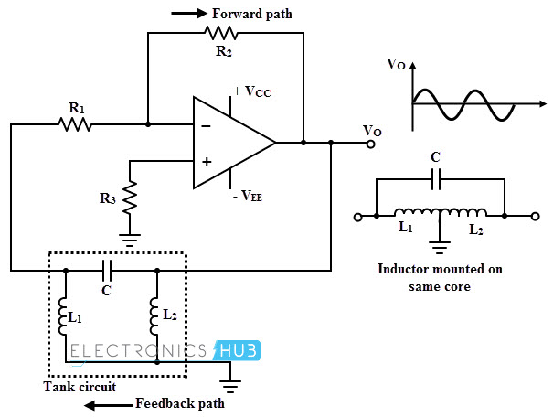
The operation of this circuit is similar to the transistor version of Hartley oscillator. The sine wave generated by the feedback circuit is coupled with the op-amp section. Then this wave is stabilized and inverted by the amplifier.
The frequency of the oscillator is varied by using variable capacitor in the tank circuit keeping the feedback ratio and amplitude of the output constant for over a frequency range. The frequency of oscillations for this type of oscillator is same as that of above discussed oscillator and is given as
fo = 1/ (2π √ (Leq C))
Where Leq = L1 + L2 + 2M or L1 + L2
To generate the oscillation from this circuit, the amplifier gain must be selected greater than or at least equal to the ratio of two inductances.
Av = L1 / L2
If the mutual inductance exists between L1 and L2 because of the common core for these two coils, then the gain becomes
Av = (L1 + M) / (L2 + M)
Example 1
Consider that the transistorized Hartley oscillator consisting of the tank circuit has the capacitance of 100pF. The inductance between the collector and tapping point is 30 µH and the value of the inductance between the tapping point and the transistor base is 1 × 10⁻⁸ H. Find out the frequency of oscillation. Neglect the mutual inductance.
Given that
C = 100pF = 100 × 10-12 F
L1 = 30 µH = 30 × 10-6 H
L2 = 30 µH = 1 × 10⁻⁸ H
The frequency of oscillations for a transistorized Hartley oscillator is given by
fo = 1/ (2π √ (L1 + L2) C))
= 1/ (2π √ ((30 × 10-6) + (1 × 10⁻⁸)) × 100 × 10-12))
= 2.9 × 10⁶ Hz
= 2.9 MHz
Example 2
Consider the given figure, in which Hartley oscillator is constructed with operational amplifier and feedback LC network. By referring the given values determine the operating frequency and maximum acceptable value of resistance R for oscillations to start.
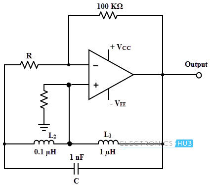
For Hartley oscillator, the frequency of oscillations is given by
fo = 1/ (2π √ (Leq C))
Where Leq = L1 + L2
Leq = 1.0 × 10⁻⁶ + 0.1 × 10⁻⁶
Leq = 1.1 × 10⁻⁶
The given capacitor value is C = 1 × 10⁻⁹ F
Therefore, fo = 1/ (2π √ (1.1 × 10-6 × 1 × 10-9)
= 4.799 MHz.
Feedback factor = L2 / L1
= 0.1 × 10⁻⁶ / 1.0 × 10-6
= 0.1
Therefore the minimum gain required = 10
But, gain= R2/R = 100 × 103/ R
Therefore, the maximum value of R = 100 × 103 / 10
= 10 K ohm.
Advantages
- Instead of two separate coils as L1 and L2, a single coil of bare wire can be used and the coil grounded at any desired point along it.
- By using variable capacitor or by making core movable (varying the inductance), frequency of oscillations can be varied.
- The amplitude of the output remains constant over the working frequency range.
- Very few components are needed including either two fixed inductors or a tapped coil.
Disadvantages
- It cannot be used as low frequency oscillator since the value of inductors become large and size of the inductors becomes bulky.
- The harmonic content in the output of this oscillator is very high and hence it is not suitable for the applications which require pure sine wave.
