Overview
In this project/tutorial, I’ll show you how to design and develop a PCB for ESP8266 WiFi Module. If you remember in the “GETTING STARTED WITH ESP8266 AND ARDUINO” project, I have mentioned that the pins of the ESP8266 WiFi Module are not breadboard friendly.
There, I have made a small perf board for ESP8266 WiFi Module in order to insert it in the breadboard, you could call it a Breadboard Adapter.
Even though this perf board served the purpose of using the ESP8266 on a Breadboard, I still had to connect the level converter resistors, push button to reset the module separately.
So, instead of making a PCB for breadboard adapter, I have decided to make a PCB for the ESP8266 WiFi Module with all the required components like connectors for power, GPIO Pins and communication (RX and TX), slide switch for selecting Programming Mode or Normal Mode, Push button for Reset, headers to insert the ESP8266 WiFi Module and the level converter resistors for the RX Pin of the Module.
Let us start the PCB for ESP8266 WiFi Module by taking a look at the circuit diagram with all the necessary components.
Circuit Diagram
Before proceeding with the PCB Design of the ESP8266 Board, you need to design the circuit diagram with all the components and connections.
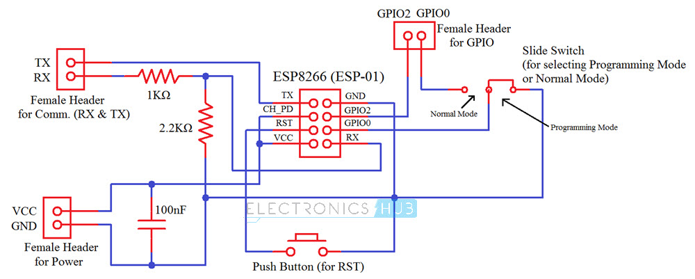
The following image shows the circuit connections with respect to the ESP8266 ESP-01 WiFi Module.
I’ll explain the design of the circuit later but first, let us see all the components that are used in the design of the circuit.
Components Required
The following is the list of all the components used to design the circuit of the ESP8266 WiFi Module PCB Board.
- ESP8266 WiFi Module (ESP-01)
- Female Headers (a few strips)
- Push Button
- 1 KΩ Resistor (1/4 Watt)
- 2.2 KΩ Resistor (1/4 Watt)
- 100 nF Capacitor
- Two Way Slide Switch
Circuit Design
First of all, we need to recollect the Pin Configuration of the ESP8266 WiFi Module. The ESP8266 ESP-01 variant has 8 pins, namely: VCC, GND, RX, TX, GPIO0, GPIO2, RST and CH_PD. The pin description is already mentioned in the earlier tutorials.
Coming to the design of the circuit, the VCC and CH_PD pins of the Module are connected to the VCC terminal of the Power Supply header, while the GND pin is connected to GND terminal.
A 100 nF ceramic disc capacitor is connected between the VCC and GND female headers.
The RST (reset) pin is connected to one end of a push button and the other end of the button is connected to GND.
GPIO2 is connected directly to one of the terminals in the female header for GPIO. The GPIO0 pin is connected to the center terminal of a two way slide switch. One end of the switch is connected to the second terminal of the female header for GPIO while the other end is connected to GND.
Next is the communication pins i.e. TX and RX. The TX pin of the ESP8266 WiFi Module is directly connected to the TX terminal of the communication female header. The RX pin on the other hand, is connected through a level converter consisting of a 1KΩ and a 2.2KΩ resistor.
Designing the PCB for ESP8266 WiFi Module
After understanding the requirements and designing the circuit diagram, you can proceed to design the PCB for ESP8266 WiFi Module. I’ve used Autodesk’s Eagle PCB Software for this purpose.
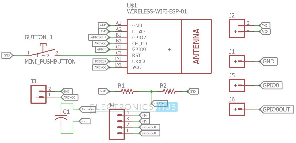
The following image shows a simple layout of the Schematic part of the PCB Design. This image is just a reference and you can draw the schematic as per your convenience using the circuit diagram.
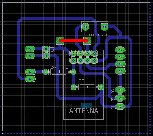
After the schematic is completed, the next step is to proceed with the actual PCB Design. Since this is a DIY PCB, I’ve used a single layer design (although I had to use a jumper at one place).
PCB layout for the ESP8266 WiFi Module is shown in the image below. Once again, this is not a great design but it serves the purpose.
Making the PCB and Assembling the Components
In the “HOW TO MAKE YOUR OWN PCB AT HOME” tutorial, I have already mentioned the necessary steps to be followed for making your own PCB. I would not repeat those steps and instruction as you follow them from that tutorial.
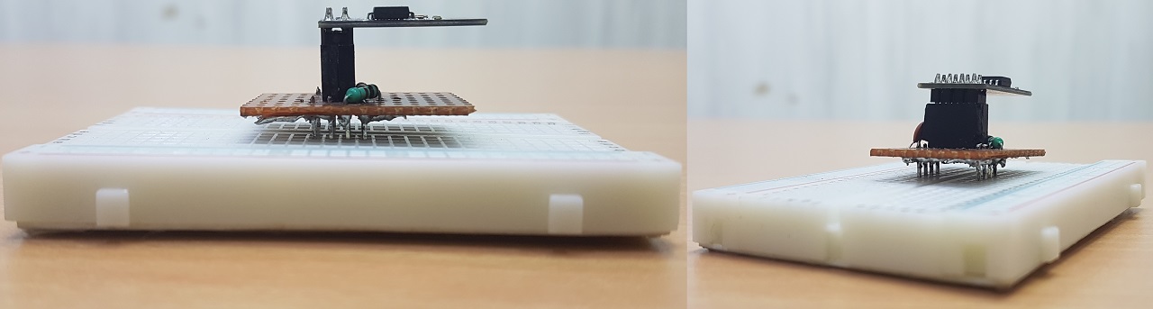
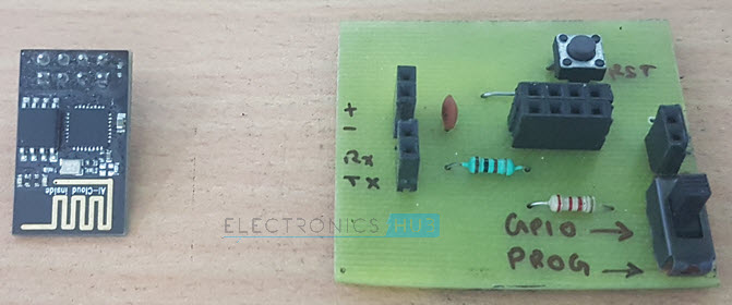
After developing the PCB, you can assemble the components and solder them on to the board. The final board with all the components placed and soldered is shown in the image below.
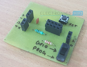
Working of PCB for ESP8266 WiFi Module
After assembling the components, connect 3.3V supply to the VCC and GND pins on the board. If you want to program the ESP8266 or flash the firmware onto it, slide the switch to Programming Mode position and press the Reset button once.
Now the programming mode is activated and you can proceed with flashing the firmware as shown in this tutorial “HOW TO UPDATE FLASH ESP8266 FIRMWARE” or just upload a blink sketch to blink an LED.
Once you are done with uploading the program/firmware, slide the switch to normal mode and press the reset button. Now the uploaded program/firmware will run.

One Response
Disconnect WiFi
How can the IC module running the WiFi transmitters in a typical broadband to ethernet/phone hub be identified? What typical IC’s are they and how easy would it be to disconnect the power to them?
Generally there is no provision to switch the WiFi transmitters off – 2.4GHZ and 5GHz – except by programming via the net, but that still leaves the carrier frequencies and power consumption – the heatsink driving the WiFi gets quite hot! Disconnecting the aerials reduces the range but not the power consumption.
One would think that the WiFi would be optional considering the security issues, but it’s not!
At least there should be a switch to turn the whole transmission system off!
Cheers