In the previous tutorial, I have shown you briefly on How to Design PCB using Eagle CAD. In this tutorial, which is a sequel to the previous one, I’ll show you How to Make Your Own PCB at Home.
We have already seen how to get started with Autodesk’s Eagle CAD Software, draw the schematic for a project (Fire Alarm Circuit) and finally draw the PCB layout using Eagle.
After checking for errors (DRC – Design Rule Check), there are two ways you can proceed with the actual PCB manufacturing: using the generated Gerber Files, you can contact any PCB manufacturing companies or PCB Houses and get your PCB Manufactured (and even assembled) or you can make your own PCB at home.
Before proceeding with making your own PCB, check out this article on How to Design PCB using Eagle CAD.
PCB Manufacturing Houses vs Making PCB at Home
Using PCB Houses is a good idea if you are developing commercial products. Usually, PCB Houses will manufacture in large quantities (to reduce the cost) and if you are ordering PCBs just for prototyping, then it might cost you more.
NOTE: The cost of manufacturing a PCB will depend on the PCB House you choose. Now-a-days, many PCB Manufacturing Companies are providing low cost but good quality PCBs for prototyping. Feel free to check them out.
An alternative to manufacturing PCBs from PCB Houses is to make one yourself at home. Making PCBs at home is a good idea if your design is simple (usually a single layered board) and if you are ready to get your hands dirty (literally).
If you have a small circuit or design that you want to try out with a PCB, then you probably can make one yourself at home without the involvement of Gerber Files, PCB Manufacturing Houses or waiting for the ordered PCB to arrive at your doorstep.
In this tutorial, I’ll show all the necessary steps on how to make your own PCB at Home using simple components and tools.
How to Make Your Own PCB at Home?
Warning: Before proceeding with the process, I suggest you to take necessary safety precaution like using goggles, gloves, mask etc.
Printing the PCB Layout on a Paper
After completing drawing the PCB layout of the circuit, we need to print the layout on a paper. To print the layout, first click on the Print Option. You will get a new window with options for setting up the print layout.
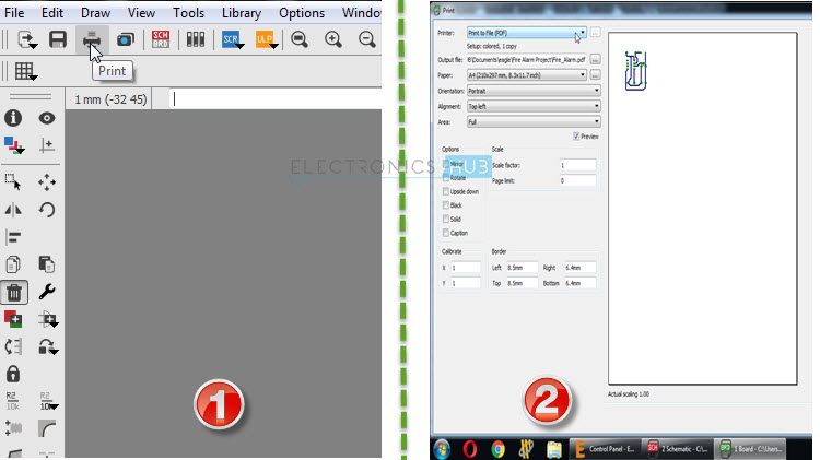
Now, in this window, set the following options.
- Printer: Print to File (PDF)
- Output file: *set the name and location of the output PDF*
- Paper: A4
- Orientation: Portrait
- Alignment: Top Left (*anywhere*)
- Area: Full
Also set the Scale Factor to 1 and Page limit to 0. Check the boxes “Black” and “Solid”. Finally click OK.
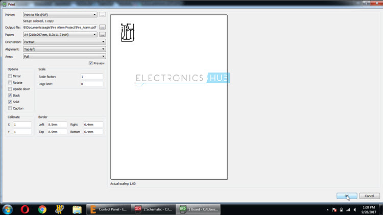
A PDF will be created in the desired location. Now, we have to print this PDF on a special paper and selecting the paper is an important task.
How to Select the Paper for PCB?
The method we are going to use for making the PCB is called Toner Transfer Method. In this method, we will take a print of the PCB Layout on a piece of special paper using Laser Printer and transfer the Toner from the paper on to the PCB board using heat transfer (iron box).
Since laser printers use toner (a type of powder) to print on the paper, the toner powder will not be absorbed by the paper but rather sticks on the surface. This is in contrast to regular inkjet printers, which use ink, to spray the print on the paper (which will be absorbed by the paper).
Hence, selecting the right paper for PCB Toner Transfer Method is very important. For this, we will use (and I suggest you use the same) a single sided Glossy Paper for Laser Printers with thickness of 130 GSM.
NOTE: Do not use Inkjet Glossy Paper with Laser printer as it might damage the drum in the laser printer.
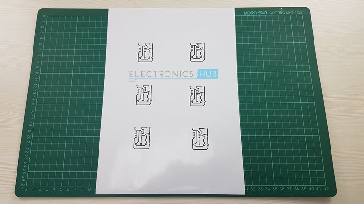
Getting the Board Ready for Toner Transfer
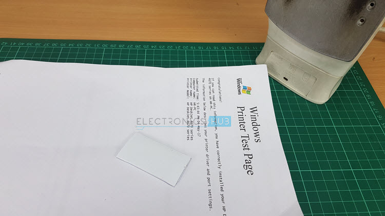
First, print the layout on the paper using laser Printer. Here, we have made multiple copies of the layout just to demonstrate that we can make multiple boards with a single paper (Save Paper!!!).
NOTE: While printing, set the paper size to A4, orientation to Portrait and check the Actual Size option (IMPORTANT).
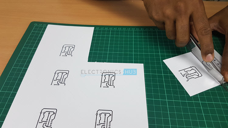
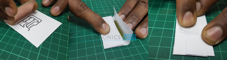
Now, cut the piece of paper with layout printed on it. Select the size of the paper a little bit larger than the final size of the board so that you can wrap the paper around the board.
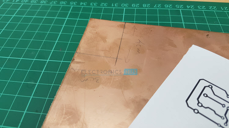
Take a Copper Clad PCB Board and mark the size of the board on one corner. In our case, it was a rectangle of size 4cm x 3cm.
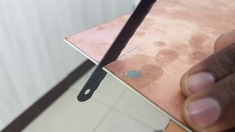
Cut the small board using a saw. Before cutting the board with saw, use a sharp tool like a box cutter and make fine groves on the surface. This will allow you to easily cut the board using the saw.
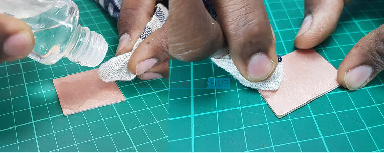
Now, the surface of the board (the one we just cut) is not clean with deposits of fingerprints and dirt. So, in order to clean the surface, use a mild emery paper or sand paper and rub it on the Copper side of the board.
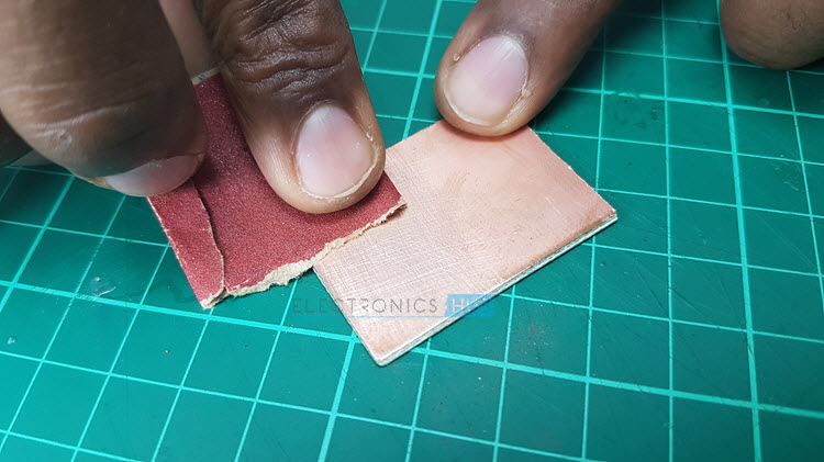
Make sure that the sand paper is not hard as it might completely remove the copper. A clean board with the surface dirt removed will look very shiny.
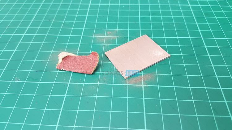
Now, clean the Copper side of the board with alcohol. If you do not have alcohol, you can use Acetone (also available as nail paint remover). This step will completely remove the small deposits of Copper Powder (caused by rubbing with sand paper) and dirt from the surface of the board.
Now, take the Copper Board and place it on the paper with the layer print facing the Copper side. Wrap the board with the extra paper we have and seal it tightly with glue or adhesive tape.
Transferring the Toner from Paper to PCB
The next step is to transfer the toner from the paper on to the Copper side of the board. For this, I’ll be using an Iron Box. There is another method of transferring the toner from paper to board called Heatless Toner Transfer, which uses chemicals to achieve the action. We will leave it to another tutorial for now.
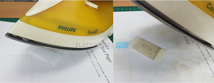
Preheat the Iron Box to around 2000C (or place the knob between cotton and linen).
Place the copper side of the board on the top and place the iron box on the board and slow start ironing the board. Apply slight pressure on the board for about 10 minutes and take of the iron box. You can see a change in color of the paper before and after ironing.
Place the board (with paper still wrapped around it) in a bowl of water. Be careful when touching the board as it might be very hot (High school Physics: Copper is a good conductor of heat!!!).
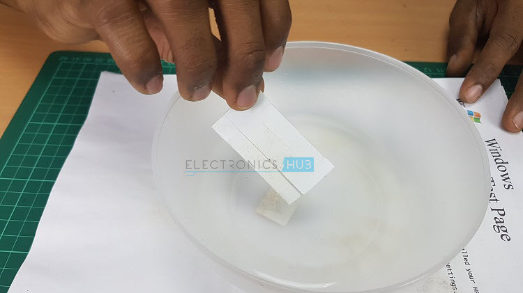
This instant cooling will bind the toner more strongly on to the Copper board. Let the board cool down for a minute or two.
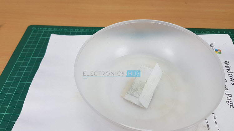
Now, you can slowly start to unwrap the paper from the board. You can notice that the paper is firmly struck to the board.
Use the water from the bowl and rub off the paper from the board. Do not apply too much pressure while removing the paper.
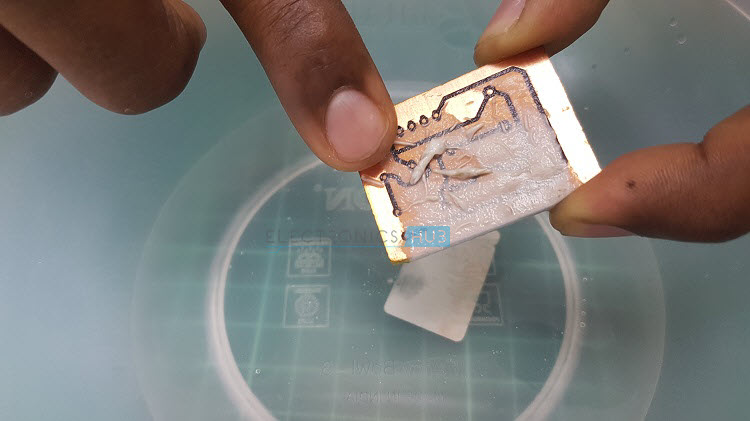
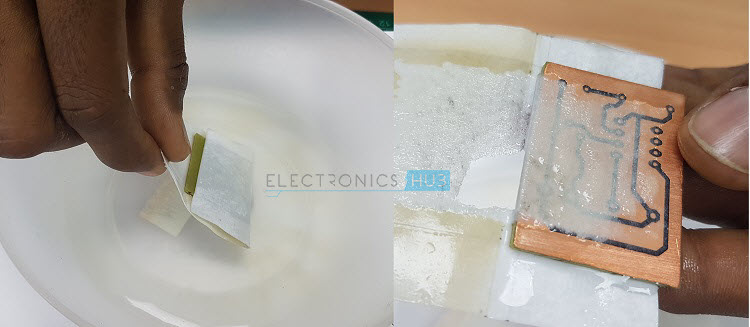
When the paper is completely removed, you can see a clean transfer of the toner on the Copper Clad Board.
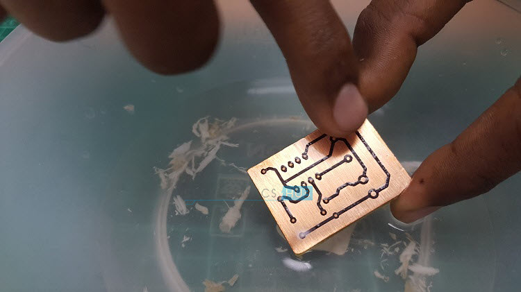
In case you feel that a part of the trace or pad did not transfer perfectly, use a permanent marker and draw on the broken or unclear toner. In our case, the transfer was very good. You can also use a multimeter to check for connectivity.
Etching the Copper from Board
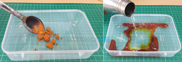
The next step is to remove all the unnecessary copper from the PCB Board. This process is called Etching. For this, I’ll be using Ferric Chloride (FeCl3). Ferric Chloride is a very harmful and toxic chemical. Be extremely careful when using it for making PCB.
Take a spoon or two of Ferric Chloride Powder and put it in a thick plastic or steel container. Pour some hot water in the container.
Warning: You can see fumes coming out of the container as soon as you add the water.
Drop the PCB in the container and stir the water for 10 to 15 minutes (or until the Copper is completely etched).
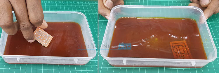
Ferric Chloride will not react with Carbon (which is the main component in the toner) but only with the Copper. Hence, the Copper on the board, except that beneath the toner (which acts as a protective layer) will be completely removed.
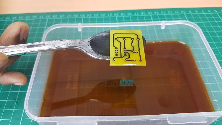
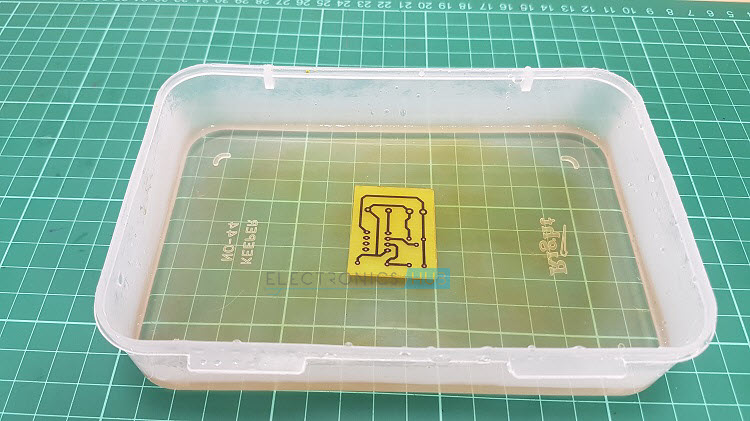
Dispose of the water carefully and add fresh water in the container. Now, place the PCB in the water to clean of the surface from chemical deposits.
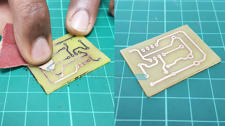
Take another piece of mild emery paper and slowly clean the toner from the PCB.

Your PCB is ready (well, almost. You still need to drill holes).
Drilling Holes on the PCB
Next step is to drill holes on the PCB to mount the components. We used a small hand drill (motorized drill) to make the holes.
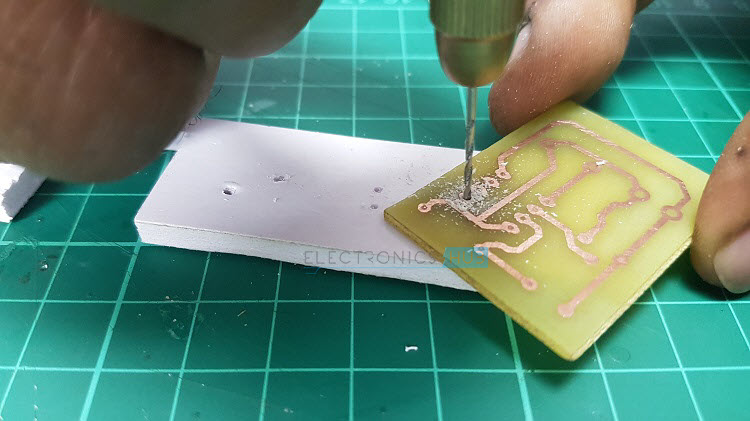
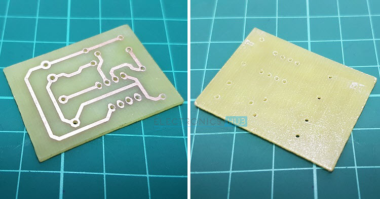
Once all the holes are drilled, your PCB is ready for assembly.
PCB Assembly
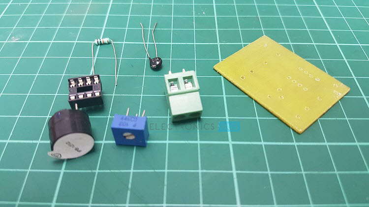
Collect all the components required for assembling on the PCB.
Place all the components in their respective positions and check if all the holes, tracks and pads are as expected or not.
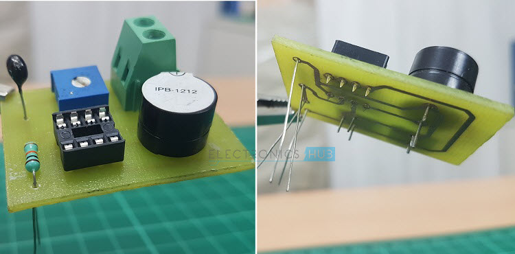
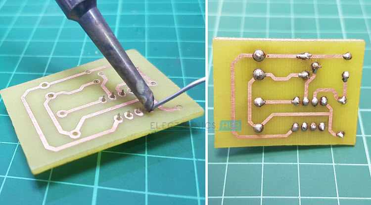
Start soldering the components on the PCB. Once done, the bottom of the board looks something like this.
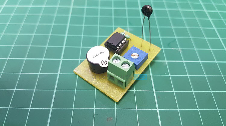
And this is the final PCB with all the components assembled.
In this tutorial, you have seen a step – by – step tutorial on how to make your own PCB at home using toner transfer method. Feel free to comment if you have made a similar board or any suggestions to the other readers.
PCBGOGO Quickturn PCB Fabrication & PCB Assembly Manufacturer
With over 10 years as an industry leader, PCBGOGO is one of the most experienced PCB and PCB assembly manufacturer in China. We are proud to manufacture high-quality PCBs and provide the best PCB assembly services for our customers. Our goal is to be categorized as the easiest Printed Circuit Board manufacturer to do business with.

14 Responses
what is the program used to implement the PCB layout
Hi, We have used Eagle CAD.
Would not it be advisable just to sand the points where the perforations and connections go, so that the tracks are protected by the toner, against oxidation?
Hi, Yes. That would be advisable. Thanks for sharing the thought. (Actually, we planned to apply solder mask but couldn’t proceed).
Actually, it would be inadvisable to leave any toner on the traces, if any heat develops in the traces or on the board, the polymer that binds the carbon component of the toner in place can melt. Well this is not common, it can eventually ignite the carbon. The carbon component of toner is a well known highly flammable component. If you wish to protect the traces, a CLEAR fingernail lacquer will work nicely provided the circuit is not used until the lacquer is completely dry.
Hi there, I never used this procedure but I will try it soon. I think it will be important to remember that the print will have to be mirrored.
I found out that a very simple and effective way of cleaning the copper without using acetone or sand paper is to rub half a lemon on it.
Very certified. ?
The application of ultraviolet laser processing in the PCB industry
I find it difficult to get a mirrored image as the many of the laser printers do not have this facility.Therefore I request you to explain if there are any methods to do this at home only as the PCB was made.
Hi. What circuit is this? It seems a temperature detector with 555. Is it?
Thank you.
Many thanks
can u please send pcb ckt for fixed bais of bjt
I do not have a laser printer.
Therefore could I make a normal inkjet print at actual size and have it copied on the glossy paper by a local photocopier shop. ?