Arduino has been the go-to platform for many makers, hobbyists, students to use in their electronics projects. Even though there are several Arduino boards, the Arduino UNO is the most popular one. The heart of this Arduino UNO board is the ATmega328P Microcontroller. So, in this guide, let us take a quick look at this microcontroller and check out its specifications. We will also see the ATmega328P Pinout and also tabulate the pin description.
Introduction to ATmega328P Microcontroller
The ATmega328P is an 8-bit microcontroller based on the AVR Architecture. While Atmel originally developed this microcontroller, it is now part of the Microchip Technology.
This IC is very famous for being the main microcontroller in several Arduino Boards such as the Arduino UNO, Arduino Nano (currently in production) and Arduino Pro Mini (retired).
It has 131 instructions, most of which execute in a single clock cycle. So, with its 16MHz clock frequency, you can expect a throughput of nearly 16 MIPS from ATmega328P (as it has 1 MIPS/MHz throughput).
Memory wise, it has 32KB of Flash Memory, 2KB SRAM and 1KB EEPROM. We will see some other specifications in the next section.
Important Specifications of ATmega328P
We have already seen couple of important specifications of ATmega328P in the previous section. Here are some more specifications for your reference.
- 8-Bit AVR Microcontroller
- Modified Harvard RISC Architecture
- 32KB Flash Memory
- 1KB EEPROM
- 2KB SRAM
- Two 8-bit Timer/Counters
- One 16-bit Timer/Counter
- Six PWM Channels
- Eight 10-Bit ADC Channels in 32-lead QFP and 32-pad QFN Packages
- Six 10-Bit ADC Channels in 28-pin DIP and 28-pad QFN Packages
- USART, SPI and I2C Interfaces
- Watchdog Timer, Pin Change Interrupt and Wake-up
- Power-on Reset, Internal and External Interrupts
- Operating Voltage:1.8V to 5.5V for 0 – 4MHz, 2.7V to 5.5V for 0 – 10MHz and 4.5V to 5.5V for 0 – 20MHz speed grades.
- Active Mode Power Consumption of 0.2mA at 1.8V and 1MHz
- Power Down Mode Consumption of 0.1µA at 1.8V and 1MHz
As always, these specifications are just for reference only. For more in-depth details on all the specifications, we suggest you to go through the datasheet.
ATmega328P Pinout and IC Packages
The ATmega328P is available in 4 IC Packages. The pinout and pin configuration slightly vary between the packages.
- 32-Lead TQFP (Thin Quad Flat Pack with Leads)
- 28-Pin SPDIP (Shrink Plastic Dual In-Line Package)
- 32-Pad VQFN (Very Thin Quad Flat No-Leads)
- 28-Pad VQFN (also known as MLF – Micro Lead Frame)
In the following image, we put out all the four packages of ATmega328P. The image also shows the ATmega328P Pinout of all the packages.
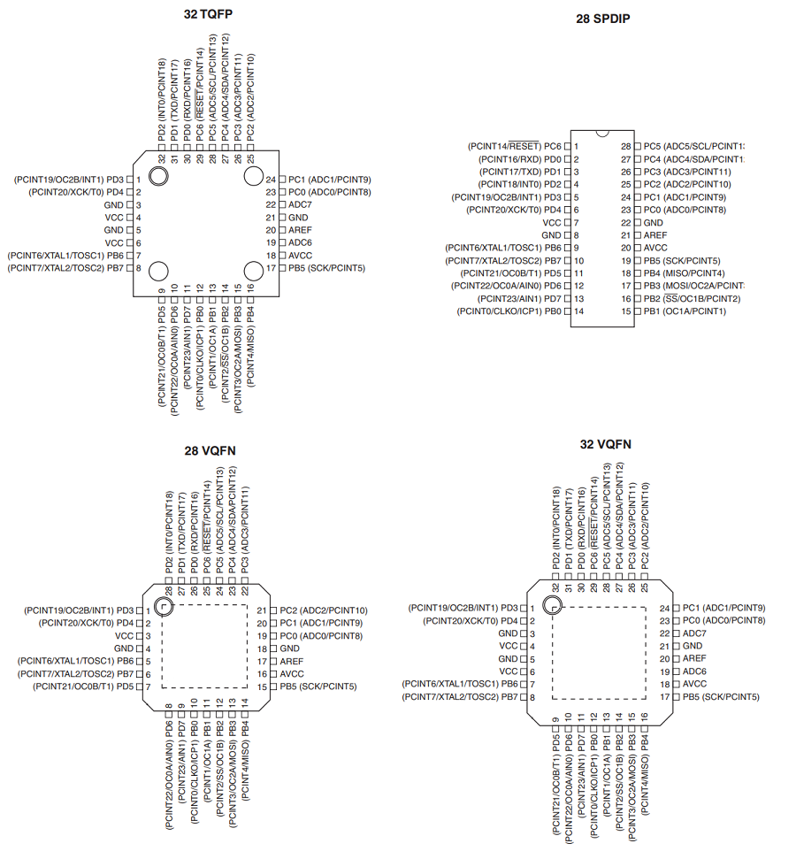
An important point to note here is that the ATmega328P Pinout for each package is different i.e., Pin 1 in 28-pin DIP is PC6 while it is PD3 in 32-lead Quad Flat Package. So, keep an eye on the package you are using and understand its pinout properly.
Also, both the 32-lead QFP and 32-pad QFN packages have same pinouts. The main difference between all these packages is that the 32-pin packages (QFP and QFN) have two additional ADC Channels (ADC6 and ADC7) than the 28-pin packages (DIP and QFN), which have only 6 ADC Channels (ADC0 to ADC5).
Other than this, rest of the pins and their alternative functions are same.
ATmega328P Pin Description
Let us now see the pin description of ATmega328P. For this section, we will use the 32-Pin QFP package as reference. So, in the following table, when we say “Pin 1”, this only refers to 32-Pin QFP package of ATmega328P only.
For other packages, the pin number might change, but the pin names, alternate functions and the overall pin description will remain the same.
| Pin Number | Pin Name | 1st Function | 2nd Function | 3rd Function | Description for Alternate Functions |
| 1 | PD3 | INT1 | OC2B | PCINT19 | External Interrupt 1 Input,
Timer/Counter2 Output Compare Match B Output, Pin Change Interrupt 19 |
| 2 | PD4 | T0 | XCK | PCINT20 |
Timer/Counter 0 External Counter Input, USART External Clock Input/Output, Pin Change Interrupt 20 |
| 3 | GND | – | – | – | Ground |
| 4 | VCC | – | – | – | Supply Voltage |
| 5 | GND | – | – | – | Ground |
| 6 | VCC | – | – | – | Supply Voltage |
| 7 | PB6 | XTAL1 | TOSC1 | PCINT6 | External Clock Input or Clock Oscillator Pin 1
Timer Oscillator Pin 1, Pin Change Interrupt 6 |
| 8 | PB7 | XTAL2 | TOSC2 | PCINT7 |
Clock Oscillator Pin 2, Timer Oscillator Pin 2, Pin Change Interrupt 7 |
| 9 | PD5 | T1 | OC0B | PCINT21 | Timer/Counter 1 External Counter Input,
Timer/Counter0 Output Compare Match B Output Pin Change Interrupt 21 |
| 10 | PD6 | AIN0 | OC0A | PCINT22 |
Analog Comparator Positive Input, Timer/Counter0 Output Compare Match A Output, Pin Change Interrupt 22 |
| 11 | PD7 | AIN1 | PCINT23 | – | Analog Comparator Negative Input,
Pin Change Interrupt 23 |
| 12 | PB0 | ICP1 | CLKO | PCINT0 |
Timer/Counter1 Input Capture Input, Divided System Clock Output, Pin Change Interrupt 0 |
| 13 | PB1 | OC1A | PCINT1 | – | Timer/Counter1 Output Compare Match A Output,
Pin Change Interrupt 1 |
| 14 | PB2 | OC1B | SS | PCINT2 |
Timer/Counter1 Output Compare Match B Output, SPI Slave Select Pin, Pin Change Interrupt 2 |
| 15 | PB3 | MOSI | OC2A | PCINT3 | SPI Master OUT Slave IN,
Timer/Counter2 Output Compare Match A Output, Pin Change Interrupt 3 |
| 16 | PB4 | MISO | PCINT4 | – |
SPI Master IN Slave OUT, Pin Change Interrupt 4 |
| 17 | PB5 | SCK | PCINT5 | – | SPI Master Clock Input,
Pin Change Interrupt 5 |
| 18 | AVCC | – | – | – | Supply Voltage for ADC |
| 19 | ADC6 | – | – | – | ADC Input Channel 6 |
| 20 | AREF | – | – | – | ADC Reference Pin |
| 21 | GND | – | – | – | Ground |
| 22 | ADC7 | – | – | – | ADC Input Channel 7 |
| 23 | PC0 | ADC0 | PCINT8 | – | ADC Input Channel 0,
Pin Change Interrupt 8 |
| 24 | PC1 | ADC1 | PCINT9 | – |
ADC Input Channel 1, Pin Change Interrupt 9 |
| 25 | PC2 | ADC2 | PCINT10 | – | ADC Input Channel 2,
Pin Change Interrupt 10 |
| 26 | PC3 | ADC3 | PCINT11 | – |
ADC Input Channel 3, Pin Change Interrupt 11 |
| 27 | PC4 | ADC4 | SDA | PCINT12 | ADC Input Channel 4,
I2C Serial Data Input/Output, Pin Change Interrupt 12 |
| 28 | PC5 | ADC5 | SCL | PCINT13 |
ADC Input Channel 5, I2C Serial Clock, Pin Change Interrupt 13 |
| 29 | PC6 | RESET | PCINT14 | – | Reset Pin,
Pin Change Interrupt 14 |
| 30 | PD0 | RXD | PCINT16 | – |
USART Input (Receive), Pin Change Interrupt 16 |
| 31 | PD1 | TXD | PCINT17 | – | USART Output (Transmit),
Pin Change Interrupt 17 |
| 32 | PD2 | INT0 | PCINT18 | – |
External Interrupt 0 Input, Pin Change Interrupt 18 |
Conclusion
ATmega328P is the microcontroller on the Arduino UNO Board. So, it is very important to understand the specifications and features of this IC. As Arduino is an open-source platform, you can design your own boards if you have all the information regarding the IC. One crucial data is the ATmega328P Pinout for different IC Packages. We saw images of ATmega328P IC Packages along with their pinouts. There is also a pin description with respective alternate functions.
