In this tutorial, we will learn about Operational Amplifiers in general, its characteristics, few applications and some of the important Operational Amplifier Basics.
Operational Amplifier or simply Op-amp is one of the most frequently and widely used electronic component. They are the main building blocks in Analog Circuits and are used in a wide range of consumer electronics, industrial equipment and scientific devices.
Introduction
An operational amplifier commonly known as op-amp is a two-input single-output differential voltage amplifier which is characterized by high gain, high input impedance and low output impedance.
The operational amplifier is called so because it has its origins in analog computers, and was mainly used to perform mathematical operations.
Depending on its feedback circuit and biasing, an op-amp can be made to add, subtract, multiply, divide, negate, and interestingly even perform calculus operations like differentiation and integration.
Today, op-amps are very popular building blocks in electronic circuits. Op-amps are used for a variety of applications such as AC and DC signal amplification, filters, oscillators, voltage regulators, comparators and in most of the consumer and industrial devices.
Op-amps exhibit little dependence on temperature-changes or manufacturing variations, which makes them ideal building blocks in electronic circuits.
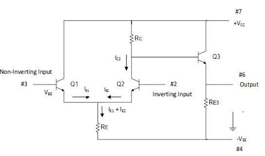
The basic circuit of an operational amplifier is as shown in the figure above. An op-amp has a differential amplifier input stage and emitter follower output stage. Practical op-amp circuits are much more complicated than the above shown basic op-amp circuit.
Transistors Q1 and Q2 forms a differential amplifier, where the difference input voltage is applied to the base terminals of Q1 and Q2. Transistor Q3 operates as an emitter follower and provides low output impedance.
The output of the basic op-amp circuit VOUT is given as,
VOUT = VCC –VRC – VBE3
VOUT = VCC – IC2RC – VBE
Where, VRC is the voltage across the resistor RC and VBE3 is the base-emitter voltage of transistor Q3.
Assume that the transistors Q1 and Q2 are matched transistors i.e., they have equal VBE levels and equal current gains. If both transistors base terminals are connected to ground, the emitter currents IE1 and IE2 are equal and both IE1 and IE2 flow through the common resistor RE. The emitter current is given by the relation,
IE1 + IE2 = VRE / RE
If both Q1 and Q2 bases connected to ground,
0 – VBE –VRE +VEE = 0
i.e. VRE = VEE – VBE
Therefore, IE1 + IE2 = (VEE – VBE) / RE
When a positive voltage is applied to the non-inverting input terminal, the base of Q1 is pulled up by the input voltage and its emitter terminal follows the input signal. Since Q1 and Q2 emitters are connected together, the emitter of Q2 also gets pulled up by the positive input at the non-inverting terminal.
The base of Q2 is grounded, so the positive voltage at its emitter causes a reduction in its base-emitter voltage VBE2 . The reduction in VBE2 causes the emitter current IE2 to decrease and consequently IC2 also reduced.
It can be noted that a positive input at pin #3 gives a positive output, hence the name non-inverting input terminal.
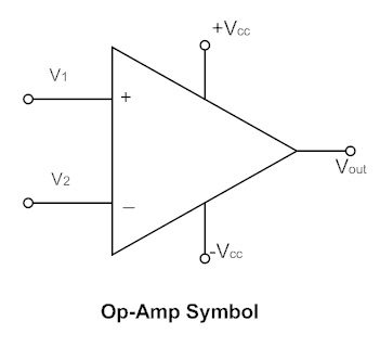
Op-Amp Symbol
Note:
- If an input signal is applied to either of the input terminals to the other input terminal connected to ground, the operation is called “single-ended”.
- In single-ended operation a single input applied, drives both the transistors due to the common-emitter connection. The output obtained is thus driven by both the collectors.
- If two input signals are applied to the two input terminals the operation is referred to as “double-ended”.
- In double-ended operation the difference of the inputs applied to the two input terminals drives the transistors and the output obtained is driven by both the collectors.
- If the same input is applied to both inputs, the operation is called “common mode”. In common-mode operation the common input signal at both the input terminals results in opposite signals at each collector.
- These signals get cancelled, resulting in an output signal zero. Practically, the opposite signals do not completely cancel each other and a small signal is resulted in the output.
Differential Amplifier using Transistors
All op-amps consist of a differential amplifier at their input stage. If two different voltage signals are applied to the two input terminals of the op-amp, the resulting output signal is proportional to the “difference” between the two signals.
Thus the differential amplifiers amplify the difference between two voltages measured with respect to a common reference. The differential amplifier stage of an op-amp is as shown below.
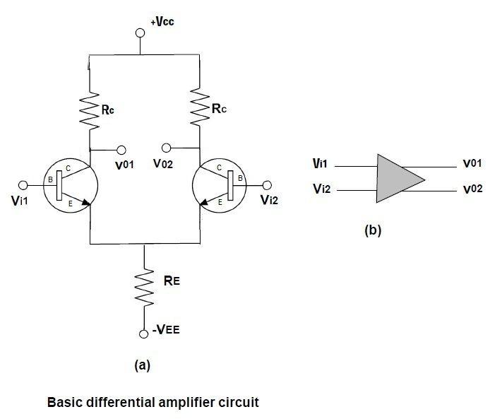
The two transistors Q1 and Q2 have identical characteristics. The two input signals Vi1 and Vi2 are applied to the base terminals of Q1 and Q2 respectively. Note that the differential amplifier has two output terminals VO1 and VO2 .
Ideally, the output voltage is zero when both the inputs are equal. When Vi1 is greater than Vi2, the output terminal VO1 will be positive and VO2 will be negative. When Vi2 is greater than Vi1, the output terminal VO2 will be positive with respect to VO1.
The output VO is given by,
VO = AD (Vi1 – Vi2)
Where AD is the differential gain.
A differential amplifier can be configured in four different ways:
- Dual input balanced output differential amplifier.
- Dual input unbalanced output differential amplifier.
- Single input balanced output differential amplifier.
- Single input unbalanced output differential amplifier.
Common Mode Gain
When the same input voltage signal is applied to both the input terminals, the operation is referred to as “common-mode” operation. The common mode signal is usually an interference or static signal.
The common mode gain is the output voltage change due to the common mode input divided by the common mode input voltage.
While a differential amplifier provides large amplification of the difference voltage applied to both the inputs, it discriminates against common mode input signals i.e. it refuses to amplify common mode signals.
The ability of a differential amplifier to reject a common mode signal is expressed in terms of its common mode rejection ratio (CMRR).
Higher value of CMRR represents its better ability to reject common mode signals. Thus any undesired signal such as noise or an interference pickup would appear as common to both the input terminals and the effect of this signal on the output would be zero.
CMRR is the ratio of differential gain to the common mode gain of the differential amplifier, i.e.
CMRR = AD /AC
Where, AD = VO / (Vi1 – Vi2)
and AC = VO(CM) / Vi(CM)
Equivalent Circuit of an Ideal Op-Amp
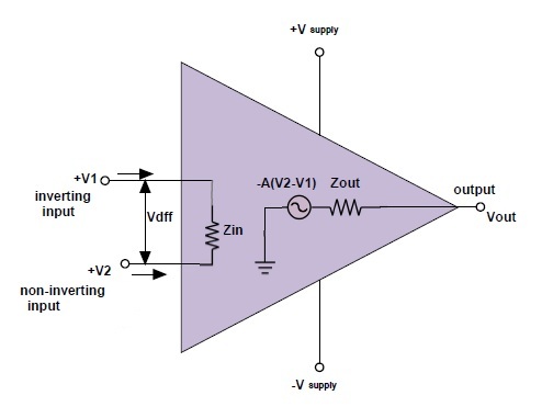
The equivalent circuit of an ideal op-amp is shown above. The input voltage VDIFF is the difference voltage (V1-V2). Zin is the input impedance and Zout is the output impedance.
The gain parameter A is called the open loop gain. If an op-amp does not have any feedback from the output to either of the inputs, it is said to be operating in open-loop configuration.
An ideal op-amp exhibits infinite open loop gain, infinite input impedance, zero output impedance, infinite voltage swing, infinite bandwidth, infinite slew rate and zero input offset voltage.
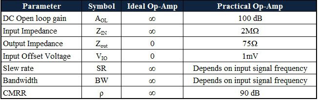
Operational Amplifier Characteristics
Input Impedance (Zin)
An ideal op-amp has infinite input impedance to prevent any flow of current from the supply into the op-amp circuit. But when the op-amp is used in linear applications, some form of negative feedback is provided externally. Due to this negative feedback, the input impedance becomes
Zin = (1 + AOL β) Zi
Where, Zin is the input impedance without feedback
AOL is the open-loop gain
β is the feedback factor (1 for voltage follower)
The impedance of the signal sources connected to the input of an op-amp must be very much smaller than the amplifier input impedance to avoid signal loss.
Output Impedance(Zout)
An ideal op-amp has zero output impedance. This means that the output voltage is independent of output current. Thus an ideal op-amp can act as a perfect internal voltage source with zero internal resistance, so that maximum current can be driven to the load.
Practically, the output impedance of the op-amp is affected by the negative feedback and is given by,
Zout = Zo / (1 + AOL β)
Where,
Zo is the output impedance of op-amp without feedback
AOL is the open-loop gain
β is the feedback factor
Load impedances connected at the output of the op-amp must be much larger than the circuit output impedance, to avoid any significant loss of output as a voltage drop across Zout.
Open-Loop Gain (AVO)
Open-loop gain of an op-amp is defined as the gain of the op-amp when there is no feedback from the output to either of its inputs. For an ideal op-amp, the gain will be infinite theoretically, but practical value range from 20,000 to 200,000.
Bandwidth (BW)
An ideal op-amp can amplify any frequency signal from DC to highest AC frequencies, thus it has an infinite frequency response. Therefore, the bandwidth of an ideal op-amp should be infinite.
In practical circuits, the bandwidth of the op-amp is limited by the gain-bandwidth product (GB).
CMRR (Common Mode Rejection Ratio)
CMRR is defined as the ability of an op-amp to reject the common mode input signal. CMRR is an important measure of an op-amp. An ideal op-amp will have infinite CMRR. In practical circuits, CMRR is given by
CMRR = 20 log10 (AD/|AC|) dB
Where, AD is the differential gain and AC is the common mode gain of the op-amp.
Offset Voltage (ViO)
The input offset voltage defines the differential DC voltage required between the input terminals to make the output zero volts with respect to ground. An Ideal op-amp will have zero offset voltage, whereas practical op-amps show some small offset.
Slew Rate
Slew rate is defined as the maximum change of output voltage per unit time and is expressed as volts per second.
An ideal op-amp will have an infinite slew rate. In practical op-amps, the slew rate is inherently limited by the small internal drive currents of the op-amp and also by the internal capacitance designed to compensate for high frequency oscillations.
Op-Amp Characteristic Table
Op-amp Frequency Response
The open loop gain AOL is not constant for all frequencies. Real op-amps have a frequency-dependent open-loop gain. The frequency response curve of a practical op-amp is as shown below.
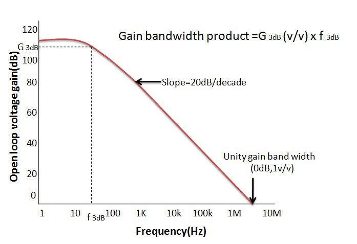
From the above curve, we can note that the product of gain and frequency is constant at any point along the curve. This constant is known as the Gain-Bandwidth product (GB). Also, the gain of the amplifier at any point along the curve is determined by unity-gain (0 dB) frequency.
Operational Amplifier Bandwidth
The bandwidth of the operational amplifier is defined as the frequency range over which the voltage gain of the amplifier is above -3dB (maximum is 0dB) of its maximum output value.
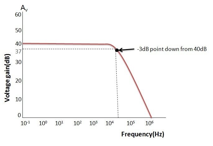
In the above figure, the -3dB of the AV(max) is shown as 37dB. The 37dB line intersects with the curve at just over 10 kHz frequencies. This frequency can be more accurately calculated if the GB product of the amplifier is known.
It can be noted that the open-loop gain decreases as the frequency of the input signal increases. Frequency is plotted in logarithmic scale and the gain decreases linearly as frequency increases in a logarithmic way.
The rate of fall of the gain in op amp is known to be 20 dB per decade.
Op-Amp Applications
- Operational amplifiers are popular building blocks in electronic circuits and they find applications in most of the consumer and industrial electronic systems.
- Op-amps can be configured to work as different types of signal amplifiers like inverting, non-inverting, differential, summing, etc. as well as it is used to perform mathematical operations like addition, subtraction, multiplication, division and also differentiation and integration.
- Operational amplifiers can be used in construction of active filters, providing high-pass, low-pass, band-pass, band-reject and delay functions.
- The high input impedance and gain of an op-amp allow straightforward calculation of element values, allows accurate implementation of any desired filter topology with little concern for the loading effects of stages in the filter or of subsequent stages.
- An operational amplifier can, if necessary, be forced to act as a comparator. The smallest difference between the input voltages will be amplified considerably.
- Op-amps are used in the construction of oscillators, like an Wein bridge oscillator. Op-amps are also used in non-linear circuits such as logarithmic and anti-logarithmic amplifiers.
- Op-amps find applications as Voltage sources, Current sources, and Current sinks and also as DC & AC Voltmeters. Op-amps are also used in signal processing circuits such as Precision Rectifiers, Clamping circuits and Sample-and-Hold circuits.
Op-Amp Summary
- An operational amplifier is a very high gain DC differential amplifier. Most op-amps require both positive and negative power supply to operate.
- Op-amps can be configured through one or more external feedbacks and voltage biases to obtain desired responses and characteristics.
- The basic op-amp construction is of a three terminal device, excluding power connections. Op-amps sense the difference between the voltage signals applied at their input terminals and then amplify it by some pre-determined gain. This gain is often referred to as the “open-loop” gain.
- Closing the open loop by connecting a resistive or reactive component between the output and one input terminal of the op-amp greatly reduces and controls this open-loop gain.
- An ideal op-amp has infinite open-loop gain, infinite input impedance, zero output impedance, infinite bandwidth, infinite slew rate and zero offset.
- A practical op-amp exhibits high open-loop gain, high input impedance and low output impedance.
- Because of their versatile uses Op-amps are used in conjunction with resistors and capacitors to build functional circuits such as Inverting, Non-inverting, voltage following, summing, subtracting, integrating and differentiating type amplifiers.

4 Responses
plz provide much more content with more deeply
what are the applications of op amps in telecom industry
Excellent. Ive never seen a better explanation.
It’s very best & easy to understand
I use to study for Linear integral circuit