Another major application of Op-amp is its use in mathematical applications. An Operational Amplifier can be configured to perform the mathematical operations of Integration and Differentiation. As a matter of fact, the name ‘Operational Amplifier’ came from the fact that it is used for performing mathematical operations. In this tutorial, we will learn and analyze the working of an Operational Amplifier as Integrator.
In the previous tutorial, we have seen how an Operational Amplifier works as a Differentiator. For more information on that topic, read “Operational Amplifier as Differentiator“.
Configuration of Operational Amplifier
Operational amplifier can be configured to perform calculus operations such as differentiation and integration. In an integrating circuit, the output is the integration of the input voltage with respect to time. A passive integrator is a circuit which does not use any active devices like op-amps or transistors but only passives like resistors and capacitors.
An integrator circuit, which consists of active devices is called an Active Integrator. An active integrator provides a much lower output resistance and higher output voltage than it is possible with a simple RC circuit.
Op-amp differentiating and integrating circuits are basically inverting amplifiers, with appropriately placed capacitors. Integrator circuits are usually designed to produce a triangular wave output from a square wave input.
Integrating circuits have frequency limitations while operating on sine wave input signals.
Ideal Operational Amplifier Integrator Circuit
An operational amplifier integrator circuit produces an output voltage which is proportional to the area (amplitude multiplied by time) contained under the waveform.
An ideal op-amp integrator uses a capacitor Cf, connected between the output and the op-amp inverting input terminal, as shown in the figure below.
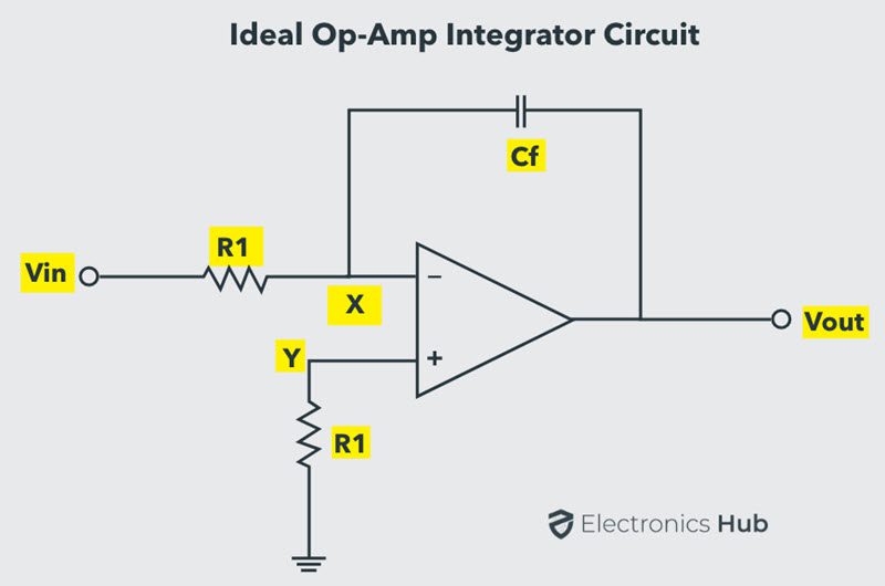
The negative feedback to the inverting input terminal ensures that the node X is held at ground potential (virtual ground). If the input voltage is 0 V, there will be no current through the input resistor R1, and the capacitor is uncharged.
Hence, the output voltage is ideally zero.
If a constant positive voltage (DC) is applied to the input of the integrating amplifier, the output voltage will fall negative at a linear rate, in an attempt to keep the inverting input terminal at ground potential.
Conversely, a constant negative voltage at the input results in a linearly rising (positive) voltage at the output. The rate of change of the output voltage is proportional to the value of the applied input voltage.
Output Voltage Calculation
From the circuit, it is seen that node Y is grounded through a compensating resistor R1. Node X will also be at ground potential, due to the virtual ground.
VX = VY = 0
Since the input current to an op-amp is ideally zero, the current flowing through the input resistor, due to Vin, also flows through the capacitor Cf.
From the input side, the current I is given as,
I = (VIN – VX) / R1 = VIN / R1
From the output side, the current I is given as,
I = Cf [d(VX – VOUT)/dt] = -Cf [d(VOUT)/dt]
Equating the above two equations of I, we get,
[VIN / R1] = – Cf [d(VOUT)/dt]
Integrating both the sides of the above equation,
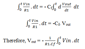
In the above equation, the output is -{1/(R1 * Cf)} times the integral of the input voltage, where the term (R1 * Cf) is known as the time constant of the integrator.
The negative sign indicates that there is a phase shift of 180o between input and output, because the input is provided to the inverting input terminal of the op-amp.
The main advantage of an active integrator is the large time constant, which results in the accurate integration of the input signal.
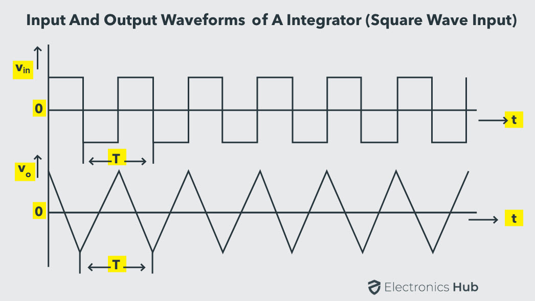
Integrator Amplifier as Ramp Generator
If the step input of the integrating amplifier is replaced by a continuous time square wave, the change in the input signal amplitude charges and discharges the feedback capacitor.
This results in a triangular wave output with a frequency that is dependent on the value of (R1 * Cf), which is referred to as the time constant of the circuit. Such a circuit is commonly called a Ramp Generator.
During the positive half-cycle of the square wave input, a constant current I flows through the input resistor R1. Since the current flowing into the op-amp internal circuitry is zero, effectively all of the current flows through the feedback capacitor Cf. This current charges the capacitor.
Since the capacitor connected to the virtual ground, the voltage across the capacitor is the output voltage of the op-amp.
During the negative half-cycle of the square wave input, the current I is reversed. The capacitor is now linearly charged and produces a positive-going ramp output.
AC Op-amp Integrator
If the Operational Amplifier Integrator is provided with a sine wave input whose frequency is varying, the integrator behaves like a “Low-Pass Filter”, which produces only low frequency signal at the output. All the high frequency signal components are blocked or attenuated.
At 0 Hz, the feedback capacitor behaves like an open-circuit, so there is no feedback from the output to the inverting input of the op-amp. Now, the circuit behaves like an open-loop inverting amplifier with very high gain.
This will result in the saturation of the output voltage. As the input frequency increases, the capacitor gets charged. At higher frequencies, the capacitor acts like a short circuit.
Op-amp Integrator with DC Gain Control
To avoid the saturation of the output voltage and to provide gain control, a resistor with high value of resistance can be added in parallel with the feedback capacitor Cf.
The closed-loop gain of the integrator will be (R2 / R1), just like a normal inverting amplifier.
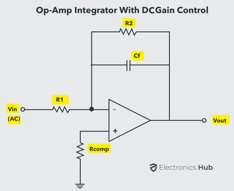
Consequently, at low frequencies of the input signal the circuit behaves normally like an integrator. At high frequencies, the capacitor acts as a short circuit and by-passes the resistor R2.
The capacitor’s reactance in turn reduces the gain of the amplifier.
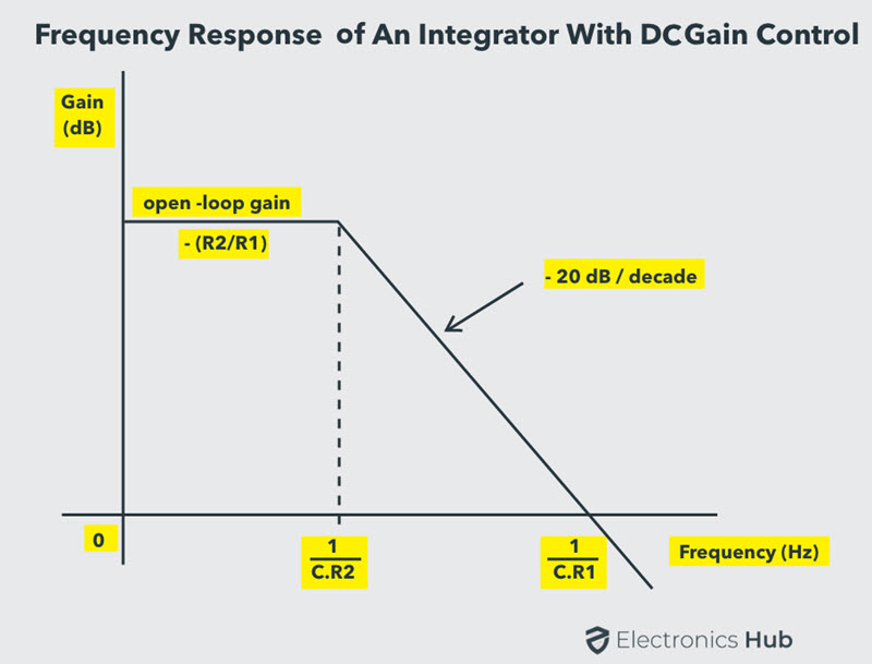
The frequency response of an AC integrating amplifier with DC gain control is as shown in the figure above. At lower frequencies of the input, the capacitor remains uncharged and acts as an open-circuit.
This results in the gain of (R2 / R1). As the input signal frequency increases, the feedback capacitor gets charged and acts almost like short-circuit, bypassing the feedback resistor R2. This results in the gain, decreasing linearly at a rate of 20 dB per decade.
Op-amp Integrator Applications
- Op-amp integrating amplifiers are used to perform calculus operations in analogue computers.
- Integrating circuits are most commonly used in analogue-to-digital converters, ramp generators and also in wave shaping applications.
- Another application would be to integrate a signal representing water flow, producing a signal representing the total quantity of water that has passed by the flow meter. This application of an integrator is sometimes called a totalizer in the industrial instrumentation trade.
Op-amp Integrator Summary
- An operational amplifier can be used to perform calculus operations such as differentiation and integration. Both these configurations use reactive components (usually capacitors than inductors) in the feedback part of the circuit.
- An integrating circuit performs the mathematical operation of integration with respect to time, on the input signal i.e., the output voltage is proportional to the applied input voltage integrated over time.
- The output of an integrator is out of phase by 180o with respect to the input, since the input is applied to the inverting input terminal of the op-amp.
- Integrating circuits are generally used to generate ramp wave from square wave input. Integrating amplifiers have frequency limitations while operating on sine wave signals.

4 Responses
Hey Therе. I found youг blog using msn. Τhis is an extremeⅼy
well written article. I’ll be sure to bookmark it and comе
back to read more ⲟf уoᥙr useful information. Thanks foг the post.
I will definitely return.
great post!
This article is very helpful and well written.Thanks and post more about op-amps and their applications in details.
Thank you a lot for giving me the opportunity to know more about op amp.
Best regards