In this tutorial, we will have a brief introduction to MOSFET i.e., the Metal Oxide Semiconductor Field Effect Transistor. We will learn about different types of MOSFET (Enhancement and Depletion), its internal structure, an example circuit using MOSFET as a Switch and a few common applications.
Transistors and its Types
Transistors, the invention that changed the World. They are semiconductor devices that act as either an electrically controlled switch or a signal amplifier. Transistors come a variety of shapes, sizes and designs but essentially, all transistors fall under two major families. They are:
- Bipolar Junction Transistors or BJT
- Field Effect Transistors or FET
To learn more about a basics of transistor and its history, read the Introduction to Transistors tutorial.
There are two main differences between BJT and FET. The first difference is that in BJT, both the majority and minority charge carriers are responsible for current conduction whereas in FETs, only the majority charge carriers are involved.
The other and very important difference is that a BJT is essentially a current controlled device meaning the current at the base of the transistor determines the amount of current flowing between collector and emitter. In case of a FET, the voltage at the Gate (a terminal in FET equivalent to Base in BJT) determines the current flow between the other two terminals.
FETs are again divided into two types:
- Junction Field Effect Transistor or JFET
- Metal Oxide Semiconductor Field Effect Transistor or MOSFET
Let us focus on MOSFET in this tutorial.
Metal Oxide Semiconductor FET
The Metal Oxide Semiconductor Field Effect Transistor (MOSFET) is one type of FET transistor. In these transistors, the gate terminal is electrically insulated from the current carrying channel so that it is also called as Insulated Gate FET (IG-FET). Due to the insulation between gate and source terminals, the input resistance of MOSFET may be very high such (usually in the order of 1014 ohms.
Like JFET, the MOSFET also acts as a voltage controlled resistor when no current flows into the gate terminal. The small voltage at the gate terminal controls the current flow through the channel between the source and drain terminals. In present days, the MOSFET transistors are mostly used in the electronic circuit applications instead of the JFET.
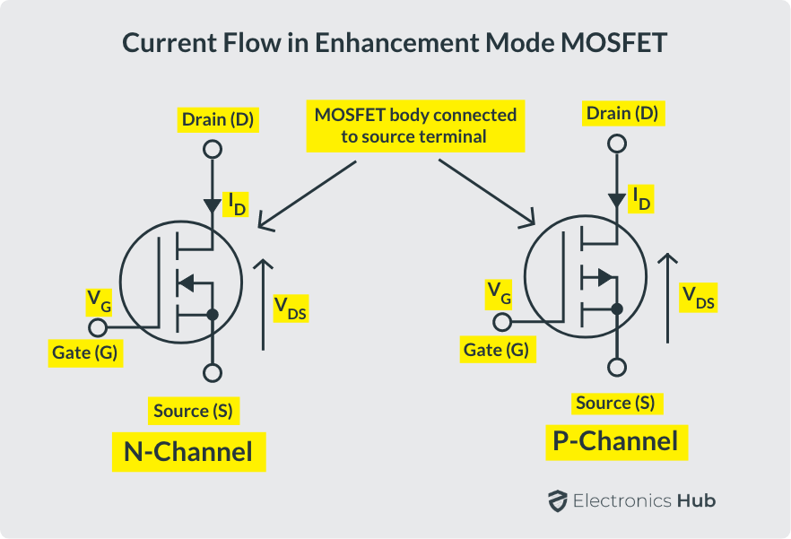
MOSFETs also have three terminals, namely Drain (D), Source (S) and Gate (G) and also one more (optional) terminal called substrate or Body (B). MOSFETs are also available in both types, N-channel (NMOS) and P-channel (PMOS). MOSFETs are basically classified in to two forms. They are:
- Depletion Type
- Enhancement Type
Depletion Type
The depletion type MOSFET transistor is equivalent to a “normally closed” switch. The depletion type of transistors requires gate – source voltage (VGS) to switch OFF the device.

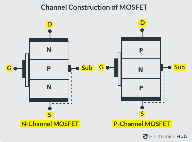
The symbols for depletion mode of MOSFETs in both N-channel and P-channel types are shown above. In the above symbols, we can observe that the fourth terminal (substrate) is connected to the ground, but in discrete MOSFETs it is connected to source terminal. The continuous thick line connected between the drain and source terminal represents the depletion type. The arrow symbol indicates the type of channel, such as N-channel or P-channel.
In this type of MOSFETs a thin layer of silicon is deposited below the gate terminal. The depletion mode MOSFET transistors are generally ON at zero gate-source voltage (VGS). The conductivity of the channel in depletion MOSFETs is less compared to the enhancement type of MOSFETs.
Enhancement Type
The Enhancement mode MOSFET is equivalent to “Normally Open” switch and these types of transistors require a gate-source voltage to switch ON the device. The symbols of both N-channel and P-channel enhancement mode MOSFETs are shown below.

Here, we can observe that a broken line is connected between the source and drain, which represents the enhancement mode type. In enhancement mode MOSFETs, the conductivity increases by increasing the oxide layer, which adds the carriers to the channel.
Generally, this oxide layer is called as ‘Inversion layer’. The channel is formed between the drain and source in the opposite type to the substrate, such as N-channel is made with a P-type substrate and P-channel is made with an N-type substrate. The conductivity of the channel due to electrons or holes depends on N-type or P-type channel respectively.
Structure of MOSFET
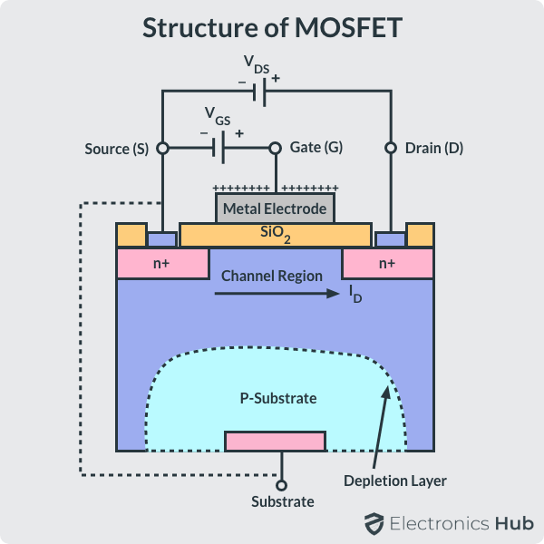
- The basic structure of the MOSFET is shown in the above figure. The construction of the MOSFET is very different when compared to the construction of the JFET. In both enhancement and depletion modes of MOSFETs, an electric field is produced by gate voltage, which changes the flow charge carriers, such as electrons for N-channel and holes for P-channel.
Here, we can observe that the gate terminal is situated on top of thin metal oxide insulated layer and two N-type regions are used below the drain and source terminals.
In the above MOSFET structure, the channel between drain and source is an N-type, which is formed opposite to the P-type substrate. It is easy to bias the MOSFET gate terminal for the polarities of either positive (+ve) or negative (-ve).
If there is no bias at the gate terminal, then the MOSFET is generally in non-conducting state so that these MOSFETs are used to make switches and logic gates. Both the depletion and enhancement modes of MOSFETs are available in N-channel and P-channel types.
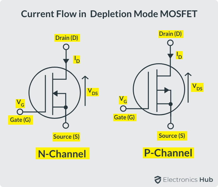
Depletion Mode
The depletion mode MOSFETs are generally known as ‘Switched ON’ devices, because these transistors are generally closed when there is no bias voltage at the gate terminal. If the gate voltage increases in positive, then the channel width increases in depletion mode.
As a result the drain current ID through the channel increases. If the applied gate voltage more negative, then the channel width is very less and MOSFET may enter into the cutoff region. The depletion mode MOSFET is a rarely used type of transistor in the electronic circuits.
The following graph shows the Characteristic Curve of Depletion Mode MOSFET.
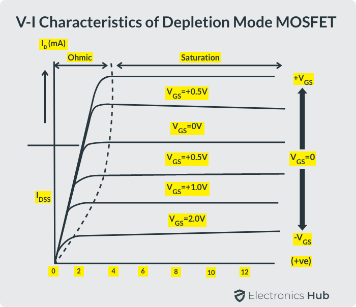
The V-I characteristics of the depletion mode MOSFET transistor are given above. This characteristic mainly gives the relationship between drain- source voltage (VDS) and drain current (ID). The small voltage at the gate controls the current flow through the channel.
The channel between drain and source acts as a good conductor with zero bias voltage at gate terminal. The channel width and drain current increases if the gate voltage is positive and these two (channel width and drain current) decreases if the gate voltage is negative.
Enhancement Mode
The Enhancement mode MOSFET is commonly used type of transistor. This type of MOSFET is equivalent to normally-open switch because it does not conduct when the gate voltage is zero. If the positive voltage (+VGS) is applied to the N-channel gate terminal, then the channel conducts and the drain current flows through the channel.
If this bias voltage increases to more positive then channel width and drain current through the channel increases to some more. But if the bias voltage is zero or negative (-VGS) then the transistor may switch OFF and the channel is in non-conductive state. So now we can say that the gate voltage of enhancement mode MOSFET enhances the channel.
Enhancement mode MOSFET transistors are mostly used as switches in electronic circuits because of their low ON resistance and high OFF resistance and also because of their high gate resistance. These transistors are used to make logic gates and in power switching circuits, such as CMOS gates, which have both NMOS and PMOS Transistors.
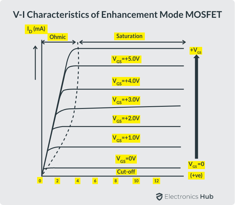
The V-I characteristics of enhancement mode MOSFET are shown above which gives the relationship between the drain current (ID) and the drain-source voltage (VDS). From the above figure we observed the behavior of an enhancement MOSFET in different regions, such as ohmic, saturation and cut-off regions.
MOSFET transistors are made with different semiconductor materials. These MOSFETs have the ability to operate in both conductive and non-conductive modes depending on the bias voltage at the input. This ability of MOSFET makes it to use in switching and amplification.
N-Channel MOSFET Amplifier
When compared to BJTs, MOSFETs have very low transconductance, which means the voltage gain will not be large. Hence, MOSFETs (for that matter, all FETs) are generally not used in amplifier circuits.
But, none the less, let us see a single-stage ‘class A’ amplifier circuit using N-Channel Enhancement MOSFET. The N-channel enhancement mode MOSFET with common source configuration is the mainly used type of amplifier circuit than others. The depletion mode MOSFET amplifiers are very similar to the JFET amplifiers.
The input resistance of the MOSFET is controlled by the gate bias resistance which is generated by the input resistors. The output signal of this amplifier circuit is inverted because when the gate voltage (VG) is high the transistor is switched ON and when the voltage (VG) is low then the transistor is switched OFF.
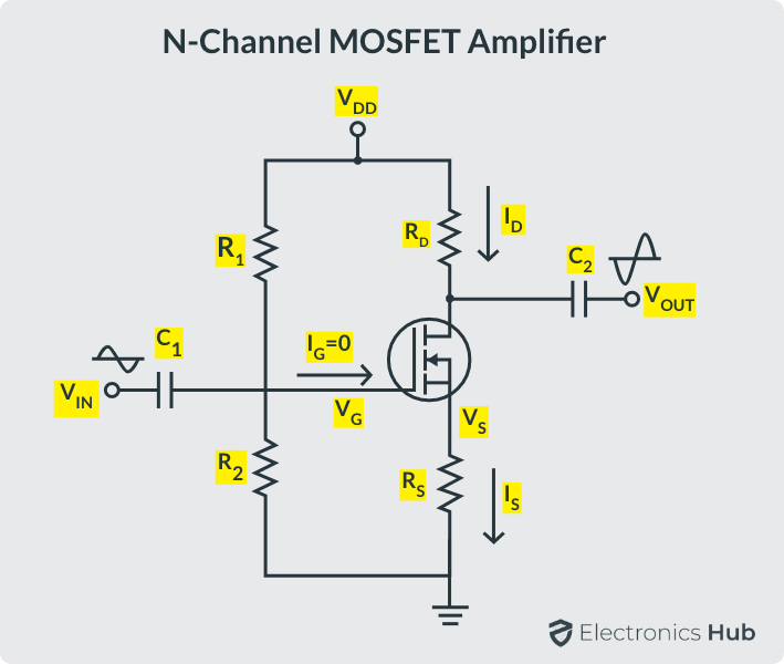
The general MOSFET amplifier with common source configuration is shown above. This is an amplifier of class A mode. Here the voltage divider network is formed by the input resistors R1 and R2 and the input resistance for the AC signal is given as Rin = RG = 1MΩ.
The equations to calculate the gate voltage and drain current for the above amplifier circuit are given below.
VG = (R2 / (R1 + R2))*VDD
ID = VS/ RS
Where,
VG = gate voltage
VS = input source voltage
VDD = supply voltage at drain
RS = source resistance
R1 & R2 = input resistors
The different regions in which the MOSFET operates in their total operation are discussed below.
Cut-off Region: If the gate-source voltage is less than the threshold voltage then we say that the transistor is operating in the cut-off region (i.e. fully OFF). In this region drain current is zero and the transistor acts as an open circuit.
VGS < VTH => IDS = 0
Ohmic (Linear) Region: If the gate voltage is greater than threshold voltage and the drain-source voltage lies between VTH and (VGS – VTH) then we say that the transistor is in linear region and at this state the transistor acts as a variable resistor.
VGS > VTH and VTH < VDS < (VGSVGS – VTH) => MOSFET acts as a variable Resistor
Saturation Region: In this region the gate voltage is much greater than threshold voltage and the drain current is at its maximum value and the transistor is in fully ON state. In this region the transistor acts as a closed circuit.
VGS >> VTH and (VGS – VTH) < VDS < 2(VGS – VTH) => IDS = MaximumThe gate voltage at which the transistor ON and starts the current flow through the channel is called threshold voltage. This threshold voltage value range for N-channel devices is in between 0.5V to 0.7V and for P-channel devices is in between -0.5V to -0.8V.
The behavior of a MOSFET transistor in depletion and enhancement modes depending on the gate voltage is summarized as follows.
| N-Channel Depletion | |||
| N-Channel Enhancement | |||
| P-Channel Depletion | |||
| P-Channel Enhancement |
Applications
- MOSFETs are used in digital integrated circuits, such as microprocessors.
- Used in calculators.
- Used in memories and in logic CMOS gates.
- Used as analog switches.
- Used as amplifiers.
- Used in the applications of power electronics and switch mode power supplies.
- MOSFETs are used as oscillators in radio systems.
- Used in automobile sound systems and in sound reinforcement systems.
Conclusion
A complete beginner’s guide to introduction of MOSFET. You learned the structure of a MOSFET, different types of MOSFET, their circuit symbols, an example circuit using a MOSFET to control an LED and also few areas of applications.

One Response
i wanna see YRANSISTOR AS SWITCH