In this tutorial, we will learn about Field Effect Transistors or FET, its working, regions of operation and see the working of a FET as a Switch. We will see both how both JFET and MOSFET can be used in switching applications.
Introduction
Wide variety of advantages such as high input impedance, simple fabrication, simple operations, etc. makes the Field Effect Transistors (FETs) to be used popularly in different applications particularly in integrated circuit systems.
FETs are the 2nd generation transistors after the BJTs. These can be used as amplifiers in oscilloscopes, testing and measuring instruments, electronic voltmeters, etc. and also used in switching actions.
Let us see in detail of the working of a FET as a switch. But before that, we have to first take a look at the basics of a FET and its operation.
FET and its Operating Regions
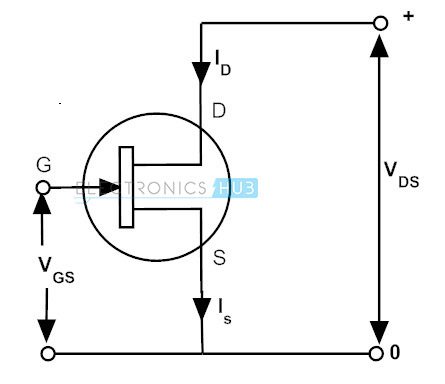
Field Effect Transistor is a unipolar device in which the current is carried only by the majority carriers (either by hoes or electrons). FET is a voltage controlled device that means, by controlling the voltage between gate and source, the output current gets varied.
Let us consider N channel JFET for understanding the operating regions. The operation or characteristics of JFET divided into three different regions, namely ohmic, saturation and cutoff region. The voltage applied to the drain is termed as VDS (some times also referred as VDD) and the voltage to the gate is termed as VGS or VGG.
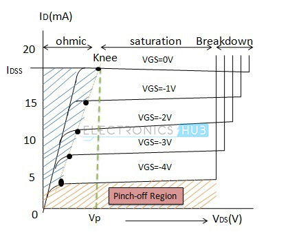
Ohmic Region (VDS> 0 and VDS < VP)
In this region channel depletion layer is very small and the FET acts as a variable resistor.
In this, the VDS value is greater than zero and less than VP so there is no pinch off of the channel and the current ID increases. When we increase the gate source voltage VGS, the channel conductance falls and the resistance is increased. Therefore, the depletion regions will spread more that makes a narrow channel. The channel resistance changes generally from 100 ohms to 10K ohms and obviously controls the voltage. Hence transistor acts as voltage controlled resistor in this region.
Saturation Region (VDS > VGS – VP )
This region starts from the point where VDS is greater than VGS minus VP, here VP is the pinch-off voltage. In this region, the drain current ID entirely depends on the VGS and not a function of VDS. The FET operates in this region to amplify the signals as well as for switching operations. From the figure it is observed that when VGS is zero, the maximum current ID flows. When we change the VGS more negative, then, the drain current is falling. At a particular value of VGS the drain current flows constantly through the device. Hence, this region is also called constant current region.
Cutoff Region (VGS < VP)
This is the region in which the drain current ID is zero and the device is OFF. In this the gate source voltage VGS is less than pinch off voltage VP. This means the value of VGS is more negative than VP. Therefore, the channel closes and doesn’t allow any current flow through the device.
FET as a Switch (JFET)
From the above discussion, it is clear that the FET can be used as a switch by operating it in two regions, they are cutoff and saturation region. When the VGS is zero the FET operates in saturation region and maximum current flows through it. Hence it is like a fully switched ON condition. Similarly, when the VGS applied is more negative than the pinch off voltage, FET operates in cutoff region and doesn’t allow any current flow through the device. Hence FET is in fully OFF condition. The FET can be used as switch in different configurations, some of these are given below.
FET Used as a Shunt Switch
Let us look at the below figure where FET is connected in parallel with the load and it acts like an analog switch.
- When the VGS applied is zero the FET is turned ON by operating in saturation region and its resistance is very small nearly 100 ohms. The output voltage across the across the FET is VOUT= Vin * {RDS/ (RD + RDS (ON))}. Since the resistance RD is very large, the output voltage is approximately considered as zero.
- When we apply the negative voltage which is equal to the pinch off voltage at the gate, FET operates in the cutoff region and acts as a high resistance device and the output voltage is equal to the input voltage.
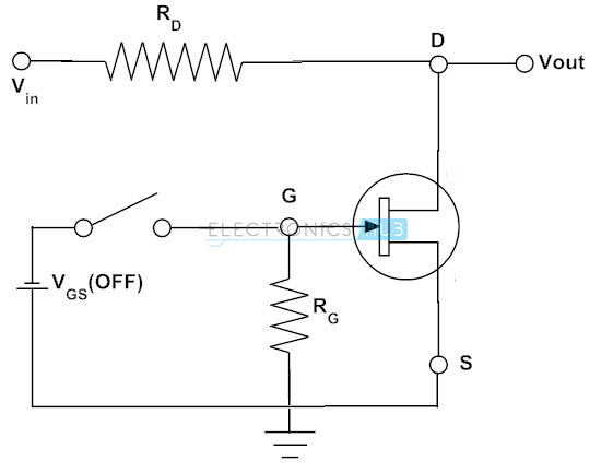
FET Used as a Series Switch
Below figure shows another configuration of FET switch circuit. In this circuit FET acts as a series switch. It acts as a closed switch if the control voltage is zero and open switch if control voltage is negative. When the FET is ON, the input signal will appear at the output and when it is OFF the output is zero.

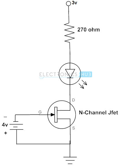
Example of N-Channel JFET as a Switch
The below figure demonstrates how a N-channel JFET used to switch the LED. The LED is connected between supply and source terminal through a resistor. Here resistor is used to limit the current through the LED. Gate terminal of the transistor connected to the negative supply.
- From the above discussion, zero voltage on the gate terminal makes current to flow through the LED because FET is in saturation mode. Therefore, the LED becomes ON.
- With a sufficient negative voltage on the gate terminal (about 3-4 volts), JFET drives into cutoff mode so the LED becomes turned OFF.
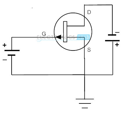
P Channel JFET as a Switch
Up to now we have discussed about N channel JFET as a switch. Another type of JFET is a P channel JFET and the operation of this FET is also similar to N-type, but only the difference is the positive voltage at the gate terminal.
- When the gate source voltage is zero the FET operates in saturation region so the FET is switched ON which in turn causes the current to flow from drain to source.
- And a positive voltage between the gate and the source causes to cut off the current through the FET. So the FET is in open circuit condition.
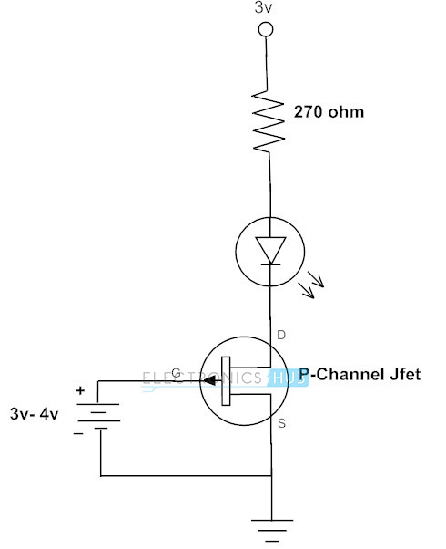
Example of P-channel JFET as a Switch
Similar to the N-channel JFET driven LED, P-channel JFET switched LED circuit is given below. The difference between the two circuits is the supply source at the gate terminal.
- Turn ON condition remains same for both circuits that is zero voltage at the gate terminal causes the LED to glow as the FET is active.
- For switching the FET into cutoff, a sufficient positive voltage (about 3 to 4 volts in this case) stops the current flow through the circuit. Therefore the LED is turned OFF. We can also use FETs for turning the relay circuits, motor drivers, and other electronic controlling circuits.
MOSFET as a Switch
Another type of FET is a MOSFET which is also a voltage controlled device. The level of VGS at which the drain current will increase or starts flowing is called threshold voltage VT. Therefore, if we increase the VGS, the drain current also increases. And if we increase the VGS by keeping the VDS constant, then the drain current will reach to a saturation level as in the case of JFET.
MOSFET operates in the cutoff mode when VGS is below the threshold level. Therefore, no drain current flows in this mode. Hence acts as OPEN switch
For a better understanding consider the below figure where N-channel enhancement type MOSFET is switched for different voltages at the gate terminal.
- In the below figure, MOSFET gate terminal is connected to VDD, so that the voltage applied at gate terminal is maximum. This makes the channel resistance becomes so small and allows maximum drain current to flow. This is called as saturation mode and in this mode the MOSFET is completely turned ON as a closed switch. For P-channel enhancement MOSFET, for turning ON, gate potential must be more negative with respect to source.
- In cutoff region, VGS applied is less than the threshold voltage level so the drain current is zero. Hence, the MOSFET is in OFF mode just as open switch as shown in figure.

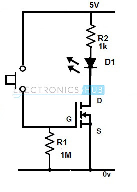
Example of MOSFET as a Switch
Let us consider the MOSFET circuit which drives the LED as shown in figure. Here N-channel enhancement MOSFET is used to switch the LED with a simple switch.
- When the switch is in open condition causes the zero voltage at the gate with respect to ground or source. So the MOSFET remains turned OFF and LED will not glow.
- When the switch is pressed to make it close, the appropriate positive voltage (5V in this case) is applied at gate terminal. so, the MOSFET is turned ON and the LED will starts glowing.
- Here it is a simple resistive load, but in case of any inductive loads like motors, relays we have to use freewheeling diodes across the load to protect the MOSFET against the induced voltages.
Most of the circuits use MOSFET as switch compared to JFET due to the advantages offered by it. We can also use switching circuit (to operate the load at particular switching frequency) for the JFETs and MOSFETs for getting the PWM signals based on the load requirements.
We hope that this overall information given might have enabled you to understand how can we switch the loads using FETs with switching conditions and necessary figures. You can also write us for any doubts or technical help on this concept in comment section below.
PREVIOUS – TRANSISTOR AS SWITCH

5 Responses
Hilarious typo: “hoes or electrons”.
This is exactly the kind of info I need,
This is the best explanation of how FETs work I’ve ever read!!! Thanks for publishing this awesome explanation of how things work!
what is the number of this mosfet to switch led used???
thanks very much