The Transistor became an essential component in modern electronics and we cannot imagine the World without Transistors. In this tutorial, we will learn about the classification and different Types of Transistors. We will learn about BJT (NPN and PNP), JFET (N-Channel and P-Channel), MOSFET (Enhancement and Depletion) and also Transistors based on their applications (Small Signal, Fast Switching, Power, etc.).
What is a Transistor?
Transistor is a semiconductor device which is used to either amplify the signals or to act as an electrically controlled switch. A Transistor is a three terminal device and a small current / voltage at one terminal (or lead) will control a large flow of current between the other two terminals (leads).
Transistors began replacing vacuum tubes decades ago due to their numerous advantages, including smaller size, better efficiency, and higher reliability. Usually, Transistors are small in size and it requires low energy for operation and also it has low power dissipation. The Transistor is one of the important active components (a device which can produce an output signal higher power than that in the input signal).
Transistor is an essential component is almost every electronic circuit like: Amplifiers, Switching, Oscillators, Voltage Regulators, Power Supplies and most importantly, the Digital Logic ICs.
From the time of invention of the first transistor to the present day, transistors are classified into different types depending either on their construction or their operation. The following tree diagram explains a Basic Classification of different Transistor types.
Transistor Tree Diagram
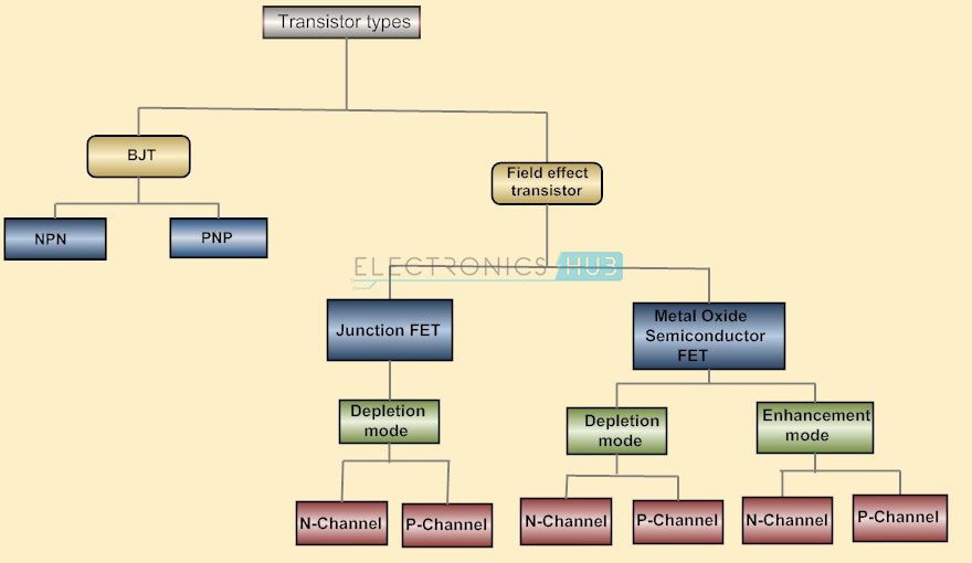
The classification of transistors can be easily understood by observing the above tree diagram. Transistors are basically classified into two types. They are: Bipolar Junction Transistors (BJT) and Field Effect Transistors (FET). BJTs are also classified into NPN and PNP transistors. The FET transistors are classified into JFET and MOSFET.
Junction FETs are classified into N-channel JFET and P-channel JFET based on their internal structure (Construction). MOSFETs are classified into Depletion Mode and Enhancement Mode. Again, depletion and enhancement mode transistors are further classified into respective N–Channel and P–Channel.
Types of Transistors
As mentioned earlier, on a broader scale, the major families of Transistors are BJTs and FETs. Irrespective of the family they belong to, all Transistors have proper / specific arrangement of different semiconductor materials. Commonly used semiconductor materials for manufacturing transistor are Silicon, Germanium and Gallium-Arsenide.
Basically, the transistors are classified depending on their structure. Each transistor type has its own characteristics, as well as advantages and limitations.
Structurally and physically, BJTs and FETs differ in such a way that BJTs need both the majority and minority charge carriers to operate, but FETs are operated with only the majority carriers.
Based on their properties and characteristics, some transistors are primarily used for switching purpose (MOSFETs) and on the other hand, some are transistors are used for amplification purpose (BJTs). Some transistors are designed for both amplification and switching purposes.
Junction Transistors
Junction Transistors are generally called as Bipolar Junction Transistor (BJT). The term ‘Bipolar’ means both electrons and holes are required for conducting current and the term ‘Junction’ means it contain PN Junction (two junctions, in fact).
The BJTs have three terminals named Emitter (E), Base (B) and Collector (C). BJTs are categorized into NPN and PNP types based on their construction.
BJTs are essentially current-controlled devices. A little current flow entering the base of a BJT initiates a large current flow from emitter to collector. The Bipolar Junction Transistors have low input impedance and it causes to flow large current through the transistor.
Bipolar Junction Transistors are switched ON only by an input current supplied to the base terminal. BJTs can operate in three regions. They are:
- Cut-off Region: Here, the transistor is in ‘OFF’ state i.e., no current passes through it. It is basically an open switch.
- Active Region: Here the transistor acts as an amplifier.
- Saturation Region: In this region, the transistor is completely ‘ON’ state and acts like a closed switch.
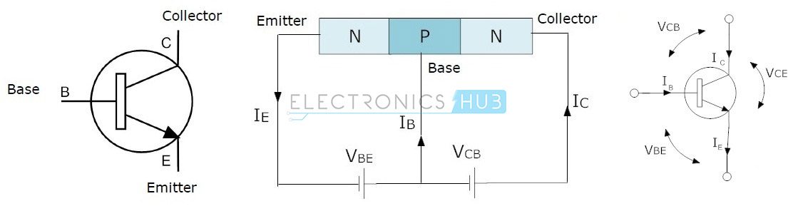
NPN Transistor
NPN is one of the two principal types of Bipolar Junction Transistors (BJTs). A transistor of NPN consists of two n-type semiconductor materials, which are separated by a thin p-type semiconductor layer. Here, the majority charge carriers are electrons while holes are the minority charge carriers. The flow of electrons from emitter to collector is controlled by the current flow in the base terminal.
A small current at the base terminal can cause a huge current flow from the emitter to the collector. Within bipolar transistors, NPN models are more popular now due to the mobility of electrons being greater than that of holes. The standard equation for the currents flowing in the transistor is
IE = IB + IC
The symbols and structure for NPN transistors are given below.
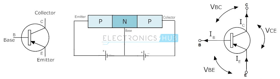
PNP Transistor
The PNP is another type of Bipolar Junction Transistors (BJT). The PNP transistors contain two p-type semiconductor materials and are separated by a thin layer of n-type semiconductor. The majority charge carriers in the PNP transistors are holes while electrons are minority charge carriers. The direction of conventional current flow is indicated by the arrow on the emitter terminal of a transistor. In a PNP transistor, the current flow will be from the emitter to the collector.
The PNP transistor is ON when the base terminal is pulled LOW with respect to emitter. The following diagram shows the symbol and structure of a PNP transistor.
FET (Field Effect Transistor)
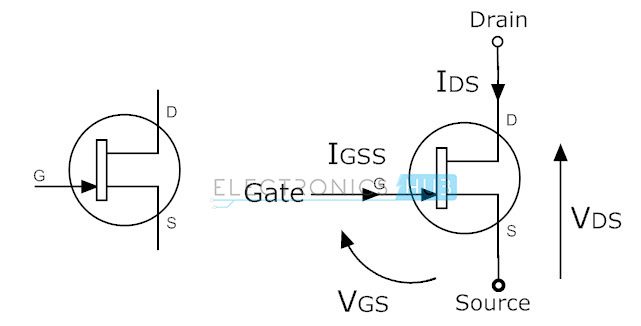
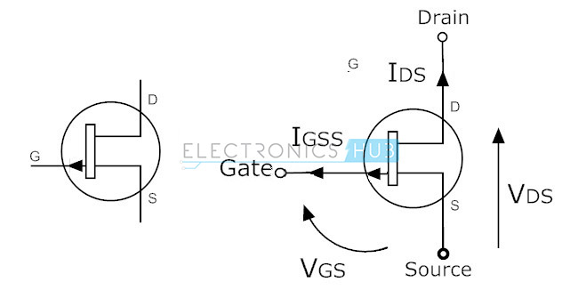
The Field-Effect Transistor (FET) is another major transistor type. Basically, the FET also have three terminals (like BJTs). The three terminals are: Gate (G), Drain (D) and Source (S). Field Effect Transistor are classified into Junction Field Effect transistors (JFET) and Insulated Gate Field Effect Transistors (IG-FET) or Metal Oxide Semiconductor Field Effect Transistors (MOSFET).
For the connections in the circuit, we also consider a fourth terminal called Base or Substrate. The FETs have control on the size and shape of a channel between Source and Drain, which is created by voltage applied at Gate.
The Field Effect Transistors are uni-polar devices, as they require only the majority charge carriers to operate (unlike BJT, which are bipolar transistors).
JFET (Junction-Field Effect Transistor)
The Junction-Field-Effect transistor (JFET) is an earliest and simple type of Field Effect Transistor. The JFETs are used as switches, amplifiers and resistors. This transistor is a voltage-controlled device. It doesn’t need any biasing current.
The voltage applied between gate and source controls the flow of electric current between source and drain of the transistor. JFETs are available in both N–channel and P-channel types.
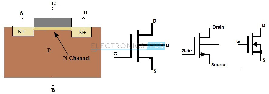
N–Channel JFET
Current is transported by electrons in an N-channel JFET. When voltage is applied between gate and source, a channel is formed between source and drain for current flow. This channel is called N–Channel. Nowadays, N–Channel JFETs are preferable type than P–Channel JFET. The symbols for N-channel JFET transistor are given below.
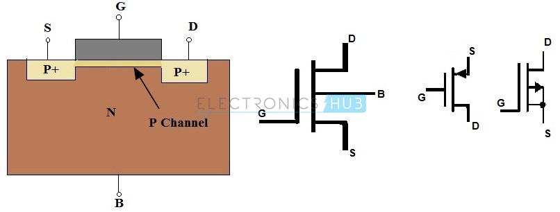
P–Channel JFET
In this type of JFET, the current flow is because of holes. The channel between source and drain is called P–Channel. The symbols for P–Channel JFETs are given below. Here, the arrow marks indicate the direction of current flow.
MOSFET
Metal Oxide Semiconductor Field Effect Transistor (MOSFET) is most commonly used and most popular type of among all transistors. The ‘Metal Oxide’ is used to describe the insulating film (thin layer of metal oxide, typically SiO₂) that separates the Gate region and the channel.
Hence, MOSFET is also known as Insulated Gate FET as the Gate region is completely insulated from the Source – Drain region. There is an extra terminal known as Substrate or Body, which is the main Semiconductor (Silicon) in which the FET is fabricated. So, the MOSFET has four terminals drain, source, gate and body or substrate.
MOSFET has many advantages over BJT and JFET, mainly it offers high input impedance and low output impedance. It is applied in switching and power circuits and acts as a main component in Integrated Circuit design technologies.
The MOSFET transistors are available in depletion and enhancement types. Further, the depletion and enhancement types are classified into N–Channel and P–Channel types.
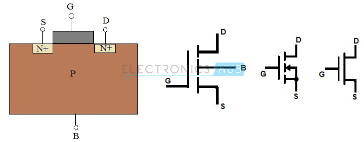
N-Channel MOSFET
An N–channel MOSFET is defined as a MOSFET that has an N-channel region between the drain and source. Here, the source and gate terminals are heavily doped with n-type materials situated in a heavily doped p-type semiconductor material (substrate).
The flow of current from the source to the drain in an N-channel MOSFET is supported by electrons. The gate voltage controls the current flow in the circuit. N–channel MOSFETs are used more often than P-channel MOSFETs because electrons are more mobile than holes.
The symbols and structures for N–Channel MOSFET transistors are given below (both Enhancement and Depletion mode).
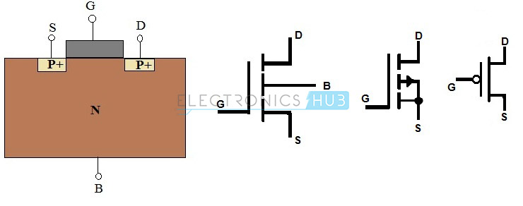
P–Channel MOSFET
The MOSFET having P–Channel region between source and drain is called as P–Channel MOSFET. Here, the source and drain terminals are heavily doped with P-type material and the substrate is doped with N-type material. The current flow between source and drain is because of holes concentration. The applied voltage at gate will controls the flow of current through channel region.
The symbols and structures for P–Channel MOSFET transistors are given below (both Enhancement and Depletion mode).
Transistors Based on Function
Transistors are also classified depending on the functions (operations or applications) they perform. Different types of transistors based on their function are explained below.
Small Signal Transistors
Small signal transistors are primarily aimed at small signal amplification, even though they can find use in switching too. These transistors are available in market in the form of NPN and PNP transistors. We can usually see some value printed on the body of small signal transistor, which indicates the hFE of transistor.
Depending on this hFE value, we can understand the capacity of transistor to amplify the signal. The commonly available hFE values are the range of 10 to 500. The collector current value of these transistors is 80 to 600 mA. This type of transistors operates with the frequency range of 1 to 300 MHz. The name of the transistor itself indicates that these transistors amplify small signals, which use small voltages and currents, such as few milli volts and milli amperes of current.

Small signal transistors are employed in almost all types of electronic equipment and are utilized in different applications, such as ON/OFF switching for general use, LED diode driver, Relay driver, Audio mute function, Timer circuits, Infrared diode amplifier, Bias supply circuits etc.
Small Switching Transistors
Small switching transistors are those transistors which are primarily used for switching but also sometimes for amplification. Similar to small signal transistors, small switching transistors come in the form of NPN and PNP and are also supplied with hFE values.
The hFE value range for these transistors is from 10 to 200. At hFE value 200, the transistors are not good amplifiers but they act as better switches. The value of collector current in them is usually between 10 mA to 1000 mA. These transistors are used mostly in switching applications.

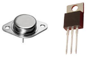
Power Transistors
The transistors which are used in the high-power amplifiers and power supplies are called as Power Transistors. The collector terminal of this transistor is connected to the base of a metal device and this structure acts as heat sink which dissipates excess power for the applications.
These types of transistors are available in the form of NPN, PNP and Darlington transistors. Here, the collector current values range from 1 to 100 A. The operating frequency range from 1 to 100 MHz. The power values of these transistors are range from 10 to 300 W. The name of the transistor itself indicates that the power transistors are used in the applications where high power, high voltage and high current are required.
High Frequency Transistors
High frequency transistors are used for small signals which operate at high frequencies and these are used in high-speed switching applications. High frequency transistors are also called as RF Transistors.
These transistors have maximum frequency values of about 2000 MHz. The collector current (IC) value ranges from 10 to 600 mA. These types of transistors are also available in the form of NPN and PNP. These are mainly used in the applications of high frequency signals and also these transistors must be ON or OFF at high speeds only. These transistors are used in HF, VHF, UHF, CATV and MATV oscillator and amplifier circuits.
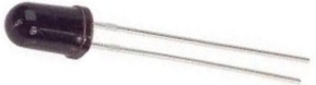
Photo Transistor
Photo transistors are the transistors which operate depending on the light i.e., these transistors are light sensitive. A simple photo transistor is nothing but a bipolar transistor which contains light sensitive area instead of the base terminal.
The photo transistors have only 2 terminals instead of 3 terminals (in BJTs). No current passes through the transistor when light is absent (dark light-sensitive area), putting the transistor in the OFF state.
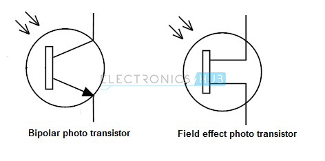
When light falls upon the light-sensitive region, a small current is produced at the base terminal, which causes a greater current flow from collector to emitter. The photo transistors are available in both BJT and FET transistor types. These are named as photo-BJTs and photo-FETs.
Unlike photo-BJTs, the photo-FETs are generating gate voltage by using light, which controls the current flow between drain and source terminals. Photo-FETs are more sensitive to light than photo-BJTs. The symbols for photo-BJT and photo-FETs are shown above.
Uni-Junction Transistors (UJT)
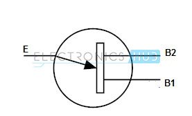
Uni-Junction Transistors (UJT) are used only as electrically controlled switches. These transistors do not contain any amplification characteristics because of their design. These are generally three lead transistors, in which, two are called as Base Terminals and the third is called the Emitter.
Now, let us see the operation of uni-junction transistor. If there is no potential difference between emitter and any one of the base terminals (B1 or B2), then a small amount of current flows between B1 and B2.
If sufficient amount of voltage is applied to the emitter terminal, then a high current is generated at emitter terminal and it adds to small current between B1 and B2, which then causes a flow of large current in the transistor.
Here, the emitter current is the primary current source for controlling the total current in the transistor. The current between the terminals B1 and B2 is very small and due to this reason, these transistors are not suitable for amplification purpose.

25 Responses
Did not mention the function about the PNP silicon transistor triple diffused
very good indroduction
GOOD EXPLANATION.
nice work
Indeed…!
it is helpful
Simple and great explained but needs little more about MOsFET
Thanku.. This is very usefull as exam poin of view.. If u have imp question related to transistor please mail me..
Good for electrical students…
It is very helpful
pls explain where to use. But very help full.
Good. But i like to ask which cause transistor to fail and how?
very helpful…
great job
Nice introduction of transistor
very helpful
A very good introduction to transistors
This is good. Thank you
You have really helped me to understand how transistors work
Wow what a good learn, I love electronics engineering because is easy to make money on that
It was a good idea about transistor.thank you all whose engaged with this idea.
I love how the transistors are explained
Very helpful thank you????
You provide very good notes.
Can I found a video about the transistors
thanks for the teaching.
An independent analysis of transistor. Good for student of Engineering.