In this article, we will see a brief Introduction to Transistors by taking a look at the predecessor to transistor i.e. the Vacuum Tubes, a history of Transistors, electrical circuit symbols of Transistors, its basis operation and also ist modes of operation.
NOTE: This will be a brush-up to the topic of transistors and won’t be too technical.
Vacuum Tubes
Before the invention of transistors vacuum tubes played a main role in electronics. Vacuum tubes are also called as electronic tubes or valves. Vacuum tube consists of an anode and the cathode.
These anode and cathode are placed in a tightly closed glass tube in which vacuum is filled. The cathode is heated by a filament which helps the cathode to emit the electrons.
In early cases, directly the cathode acts as filament, thus when this cathode is heated then electrons will emit from its surface. Later external filament which heats the cathode indirectly is introduced.
The produced electrons will flow towards the anode. This creates the potential difference between an anode and the cathode thus develops an electric current in the circuit. The filament must be continuously charged with constant power in order to heat the cathode.
To direct these electrons flow evenly towards anode external electrodes are used which are commonly called as grids. This construction makes circuit bulky and increase cost.
In early days these vacuum tubes are used in the manufacture of first generation Computers, Radios and Televisions. Later these are used for military applications and tube based audio amplifiers. But later these vacuum tubes are replaced by Transistors and Diodes.
Because the vacuum tubes are large in size, a bit expensive and consumes more power when compared with transistors. So, these restrictions of vacuum tubes are overcome by the transistors. Transistors do not require any filament current.
A Brief History of Transistors
Fed up with the large power consumption and low reliability of vacuum tubes director of research, Kelly, at bell laboratories assigned William Shockley to investigate on semiconductors to replace these tubes. John Bardeen, Walter Brattain conducted experiments under the guidance of Shockley.
William Shockley experimented on field – effect amplifier but failed. But later John Bardeen, Walter Brattain researched and discovered that electrons form a barrier on the surface which is unknown until then. This breakthrough leads to the discovery of first transistor.
In December, 1947 their experiment with two gold contacts applied to the germanium crystal produced an output signal power greater than the input signal. Thus the first transistor technology developed was known as point contact device and this technology was regulated by higher performance types. This was first reported in June, 1948.
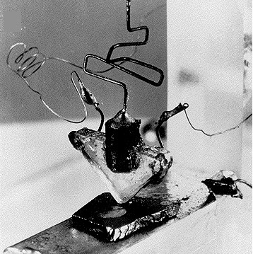
Image Resource Link: www.ece.umd.edu/class/enee312-2.S2005/
Later the limitations of point contact device, made Shockley alone, to invent junction transistor which dominated the point contact device and is easy to manufacture.
The trading of transistors started from 1950’s and first commercial transistor was used in telephonic equipment and military computers in 1952. In 1953 transistor is used in deaf aid, a medical device.
Rise of Transistors
This effective rise of transistor technology is mainly due to donation and encouragement of many companies including Bell Labs, Motorola, Philco, Raytheon, RCA, Sylvania and Texas Instruments.
In the fabrication of amplifying crystals semiconductor material plays a major role. The first transistor is made of semiconductor material, germanium in 1950s. When an electrical voltage is applied, this semiconductor material is neither fully conducting nor fully insulating.
Later silicon transistors are developed. Due to successful performance at high temperatures silicon transistor are more used from the year 1954. Commercial silicon transistors were available from Texas Instruments. Later extensive research is made from silicon transistors and now this lead to development of integrated circuit and microprocessor devices.
Later in 1959, first field effect transistor was developed. It consists of three layers metal (M-gate) ,Oxide(O-insulation ), silicon (S-semiconductor).
Initially the material used for transistor case shape is plastic epoxy. But the plastic case devices may degrade over time. So, the combinations of plastic and metal case shapes are developed in mid 1960s.
During manufacturing of a transistor, the semiconductor material is processed with the addition of small amounts of chemical impurities, such as arsenic or antimony. This process was referred as “doping”.
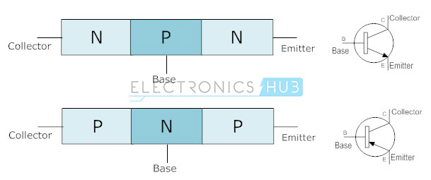
It is required in order to create proper crystalline structure in the semiconductor to allow transistor action. Depending on the doping elements used in semi-conductor material, transistors can be classified as either PNP or NPN. PNP and NPN are representations of the electrical polarity to be used with the transistor.
For example, a PNP transistor would require a specific set of Positive and Negative voltage polarities to be used for the three transistor terminals in circuit applications. NPN transistor requires all circuit voltage polarities to be reversed from those used for a PNP. Many circuit applications require the both PNP and NPN transistors.
What is a Transistor?
Transistor is symmetrical to a vacuum triode and relatively very small in size. Transistor is a composition of two words Transfer and Varistor. A transistor consists of three layers of semi conductor material and each layer is having the capability of transferring current to the other layers.
This three layer semiconductor device consisting of either two n-type and one p-type layers of material or two p-type and one n-type layers of material. First type is called an npn transistor, while the other is called a pnp transistor respectively.
Germanium and silicon are most preferable semiconductor materials which conducts electricity in semi energetic way. By the process of doping to the semi conductor material, the result adds additional electrons to the material or produce holes in the material.
The outer layers have widths much greater than the inserted p-type or n-type material that is typically in 10:1 ratio or less. Lower doping level decreases the conductivity and increases the resistance of this material, by limiting the number of free carriers.
The difference between the diode and the transistor is: A diode is made up of two layers and one junction. Transistor is made of three layers with two junctions. A transistor can acts as an on/off switch or an amplifier.
Transistor Symbols
Easy way to remember these transistor symbols is that
- PNP-Points In Permanently
- NPN-Never Points iN
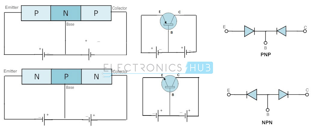
In the symbol of a transistor the arrow indicates the direction of the current flow.
The positive and negative states of voltage and direction of current flow, are always be in an opposite direction in PNP transistor with respect to NPN transistor. However the operation performed by the NPN and PNP transistors are same.
Operation Modes of the Transistor
There are four modes of operations they are saturation, cutoff, active and reverse active.
Saturation Mode
In this mode transistor acts as a switch. From collector to emitter the current will flow unconditionally (short circuit). Both diodes are in state of forward biased.
Cut-off Mode
In this mode also transistor acts like a switch but there is no current flow from collector to emitter (open circuit). There is no current flow through both emitter and collector terminals.
Active Mode
In this mode the transistor acts like an amplifier that is the current from the collector terminal to emitter terminal is corresponding to the current through the base terminal. Base will amplify the current moving into the collector terminal and outgoing from the emitter terminal.
Reverse active Mode
The current from the collector terminal to emitter terminal is corresponding to the current through the base terminal but this flow is in reverse direction.
Back to Back Connection of a Diode
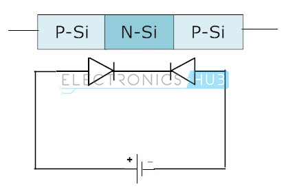
The depletion layer developed at pair of junctions namely collector-base and emitter-base of the transistor mainly due to current carriers only. In the case of two diodes connected back to back, the formed depletion region cannot pass current carries that are for both holes and electrons.
We already know that due to the thin base layer only the transistor is working and this layer is nothing but the inserted part of the emitter and collector. Due to this the emitter and collector comes very impending to each other. When strong electric field is applied then this grants the majority carriers to pass from the emitter.
These majority carriers will spread as minority carriers over the base and inside the depletion area of the junction at base-collector. In simple logic, device with one NP junction and one PN junction that acts like two diodes are placed back to back.
At this condition when we apply large voltages across the base terminal the current cannot flow through the circuit. Because the applied voltage makes one barrier large and another barrier small from which we cannot pass the current.
In order to overcome this situation besides the main voltage supply which is placed at the top of the N-P terminals a small voltage source is added at the lower P-N levels. Due to this small voltage supply it will push the electrons in to the holes part.
The main voltage supply will control the current flow. By these two actions at the depletion layer the current barriers are reduced. Thus there will be high ascending increase in the voltage through the transistor.

4 Responses
please give me few information how i can download from this channel?
I appreciate the refresher on the basics of transistor theory
Extremely well done. Pointed, precise, accurate, simplified, effective presentation. Well communicated. Rare and thank you.
This post is incredibly informative! I love the detailed history and the explanation of how transistors evolved from vacuum tubes. The inclusion of symbols is really helpful too. It’s amazing how such a small component can have such a huge impact on technology! Thank you for compiling all this information in one place!