A power amplifier circuit using MOSFET has been designed to produce 100W output to drive a load of about 8 Ohms. The power amplifier circuit designed here has the advantage of being more efficient with less cross over distortion and total harmonic distortion.
Principle of MOSFET Power Amplifier Circuit Operation:
This circuit operates on the principle of multi-stage power amplification consisting of pre amplifiers, drivers and power amplification using MOSFET. The pre amplification is done using a differential amplifier, driver stage is the differential amplifier with current mirror load and power amplification is done using MOSFET class AB operation. MOSFETs have an advantage over BJT in having a simple drive circuit, being less prone to thermal stability and having high input impedance. A pre-amplifier consisting of a two stage differential amplifier circuit is used to produce a noise free amplified signal. First stage of the pre-amplifier consists of a differential mode emitter coupled amplifier using PNP transistors. The second stage consists of a differential amplifier with active load, so as to increase the voltage gain. The current mirror circuit actually ensures the output current to remain constant irrespective of the changes in input signal voltages. This amplified signal is then given to the push pull amplifier stage, which produces a high power output signal.
Also read the post: How to Design 150W Power Amplifier Circuit
100W MOSFET Power Amplifier Circuit Diagram:
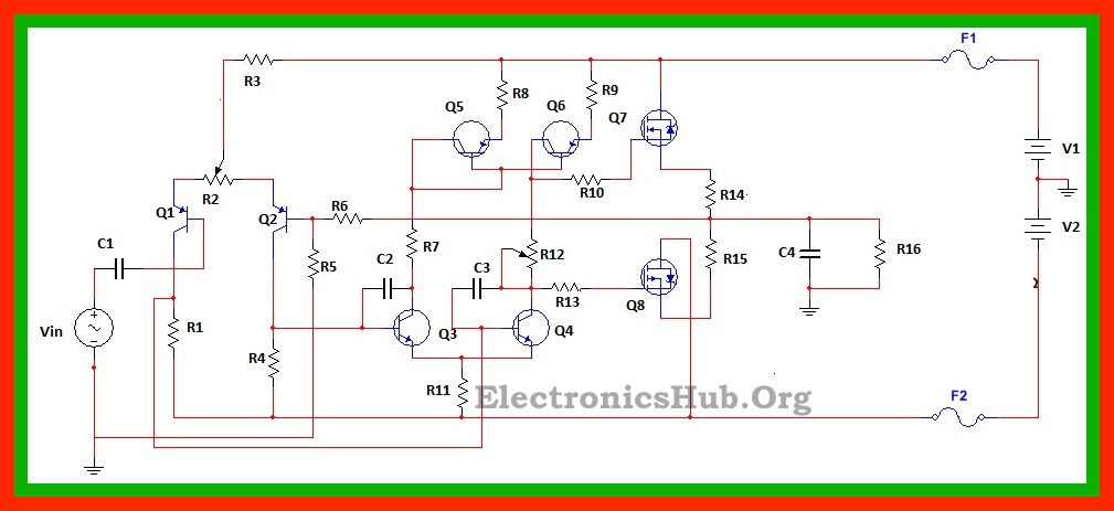
Components of the Circuit:
- R1, R4: 4k ohms
- R2: 100 ohms
- R3: 50k ohms
- R5: 1k ohms
- R6: 50k ohms
- R7: 10k ohms
- R8, R9: 100 ohms
- R10, R13: 470 ohms
- R11: 100 ohms
- R12: 3k ohms
- R14, R15: 0.33 ohms
- C1: 10uF
- C2, C3: 18pF
- C4: 100nF
- Q1, Q2: BC556, PNP transistors
- Q3, Q4: MJE340, NPN transistors
- Q5, Q6: MJE350, PNP transistors
- Q7: n channel E-MOSFET, IRF530
- Q8: p channel E-MOSFET, IRF9530
- V1, V2: +/- 50 V.
Related Post – 100w Subwoofer Amplifier Circuit
MOSFET Power Amplifier Circuit Design:
1st Stage Differential Amplifier Design:
- Selection of Emitter Resistors: For an efficient differential amplifier, the common mode rejection ratio given by R3/R2 should be higher. This requires the value of R2 to be much lower than R3. Here we select a 100 ohm potentiometer as R2 and 50k resistor as R3.
- Selection of Collector Resistors: For a differential gain of around 50 and emitter resistance about 100 Ohms, the value of R1 and R4 is calculated to be about 4k.
- Selection of Coupling Capacitor: Here we select a capacitor of 10uF to couple the AC input signal to the input of Q1.
2nd Stage Differential Amplifier Design:
- Selection of R11: For a total emitter current of around 0.5A, the value of emitter resistance is chosen to be around 100 ohms.
- Selection of R12: The value of potentiometer R12 is determined by the Gate threshold voltage of MOSFETs and the quiescent current flowing through the collector of Q4, which is around 50mA. This gives R12 to be around 3k. Similarly value of R7 is taken to be around 10k.
- Selection of Load: Here the differential amplifier is connected to an active load, which is a current mirror circuit. Here we select PNP transistors MJE350 with emitter resistors 100 ohms each. The emitter resistors are selected for a approx voltage drop of 100mV across them to ensure decent matching of the transistors.
Power Amplifier Output Stage Design:
Here we select N channel MOSFET IRF530 and P channel MOSFET IRF9530 as power amplifiers. For a power of 100w and load of 8 ohms, required output voltage is about 40V and output current is about 5A. This gives the value of source resistors to be around 0.33 ohms and the current drawn by each MOSFET to be around 1.6A (output voltage/(pi multiplied by load resistance)).
100W MOSFET Power Amplifier Circuit Operation:
PNP transistors form the differential amplifier circuit where one of the transistors receives the input AC signal and the other transistor receives the output signal through feedback. The AC signal is coupled to the base of Q1 through coupling capacitor and feedback signal is fed to the base of Q2 through R5 and R6. The output of the amplifier is set by adjusting the potentiometer. The output from the first stage differential amplifier is fed to the input of the second stage differential amplifier. When input voltage is more than the feedback voltage (in case of the first differential amplifier), the voltage inputs to the transistors Q3 and Q4 of the second differential amplifier simultaneously differs from each other. The transistors Q5 and Q6 form the current mirror circuit. This current mirror circuit ensures the output current flowing to the push pull amplifier circuit to remain constant.
This is achieved because when collector current of Q3 increases, the collector current of Q4 decreases to maintain a constant current flowing through the common point of the emitter terminals of Q3 and Q4.
Also the current mirror circuit produces an output current equal to the collector current of Q3. The potentiometer R12 ensures the application of proper DC biasing to each MOSFET. Since the two MOSFETs are in complementary to each other, when a positive voltage is applied to the gate of Q7, it conducts. Similarly for a negative threshold voltage, Q8 conducts. The gate resistors are used to prevent the MOSFET output from oscillating.
The input to the circuit is given by a 1khz AC input voltage of 4Vp-p. An oscilloscope is connected such that channel A is connected to input and channel B is connected to output. The power at the load is observed by connecting a wattmeter to the load.
Applications of 100w MOSFET Power Amplifier Circuit:
- It can be used to drive audio loads like loudspeaker, as an audio amplifier.
- It can be used to drive RF loads like high power antenna.
- It can be used to implement a distributed speaker system
- This circuit can be used in electronic devices like televisions, computers, mp3 players etc.
Limitations of this Circuit:
- MOSFET is more prone to electrostatic discharge.
- The MOSFET draws quite high current from the supply, which can damage the whole circuit, unless safety fuses are used.
- This circuit is prone to high frequency oscillations.
- This circuit is a theoretical circuit and is for education purpose.

10 Responses
nice projects . thanks you
what is F1 and F2?
Fuses, They protect the circuit to overload currents.
I don’t understand what is F1 &F2.
Can I implement this circuit for my mini project?
Nice piece .Thank alot
Very well explain with beautiful circuit diagram. Thanks.
how much is R16
nice one,
please can anyone help show me how the 100W was gotten,as it will help me create a design of any power rating of my choice
Good circuit