In this tutorial, we will learn about another important flip-flop known as the T Flip-Flop. We will learn its design, working and also couple of applications of T Flip Flop.
Design of T Flip Flop
T flip – flop is also known as “Toggle Flip – flop”. To avoid the occurrence of intermediate state (also known as the forbidden state) in SR flip – flop, we should provide only one input to the flip – flop called the Trigger input or Toggle input (T).
Then the flip – flop acts as a Toggle switch. Toggling means ‘Changing the next state output to complement of the present state output’.
We can design the T flip – flop by making simple modifications to the JK flip – flop. The T flip – flop is a single input device and hence by connecting J and K inputs together and giving them with single input called T, we can convert a JK flip – flop into T flip – flop.
So, a T flip – flop is sometimes called as single input JK flip – flop.
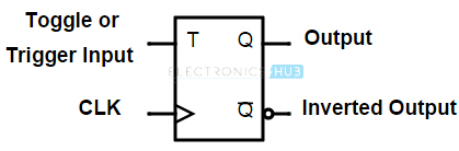
The logic symbol of T flip – flop is shown below. It has one Toggle input (T) & one clock signal input (CLK).
T Flip – Flop Circuit
We can construct a T flip – flop by any of the following methods:
- Connecting the output feedback to the input in SR flip – flop.
- Connecting an XOR with T input and Q PREVIOUS output to the Data input in D flip – flop.
- Hard – wiring the J and K inputs together and connecting it to T input in JK flip – flop.
Using SR Flip-Flop
We can construct a T flip – flop by connecting AND gates as input to the NOR gate SR latch. And one of the inputs to these AND gates are the feedback from the present state output Q and its complement Q to the respective AND gates i.e., Q to the AND Gate associated with R input and Q to the AND Gate associated with S input.
A toggle input (T) is connected in common to both the AND gates as an input. The AND gates are also connected with common Clock (CLK) signal.
In the T flip – flop, a pulse train of narrow triggers are provided as input (T) which will cause the change in output state of flip – flop. So, these flip – flops are also called Toggle flip – flops. The circuit diagram of a T flip – flop constructed from SR latch is shown below.

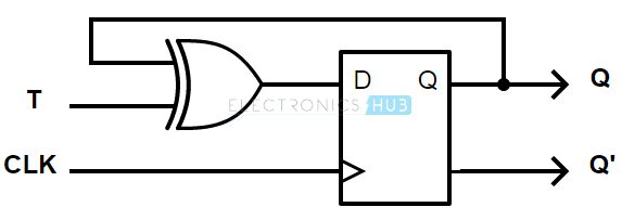
Using D Flip-Flop
Similarly, a T flip – flop can be constructed by modifying D flip – flop. In D flip – flop, the output Q is XORed with the T input and given at the D input. The circuit of a T flip – flop constructed from a D flip – flop is shown below.
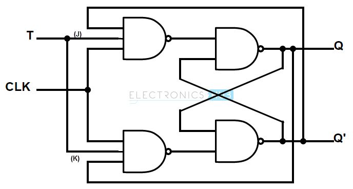
Using JK Flip-Flop
The simplest of the constructions of a T flip – flop is with JK flip – flop. The J input and K input of the JK flip – flop are connected together and provided with the T input. The logic circuit of a T flip – flop constructed from a JK flip – flop is shown below.
Working
T flip – flop is an edge triggered device i.e., the low to high or high to low transitions on the input clock signal will cause a change in the output state of the flip – flop.
Truth Table of T flip – flop
The truth table of a T flip – flop is shown below.
| Previous | Next | |||
| T | QPREV | QPREV | QNEXT | QNEXT |
| 0 | 0 | 1 | 0 | 1 |
| 0 | 1 | 0 | 1 | 0 |
| 1 | 0 | 1 | 1 | 0 |
| 1 | 1 | 0 | 0 | 1 |
As mentioned earlier, T flip – flop is an edge triggered device. For example, consider a T flip – flop made of NAND SR latch as shown below.

If the output Q = 0, then the upper NAND (NAND C) is in disable state (doesn’t have any dominating inputs) and lower NAND (NAND D) gate is in enable condition (feedback from Q is the dominating input). This means, the the Toggle Input will set the input condition for the RS Flip-Flop as R = 1 and S = 0. If you recall the truth table of RS Flip-Flop, this condition will SET the output. Hence, Q becomes 1.
If the output Q = 1, then the upper NAND is in enable state and lower NAND gate is in disable condition. This allows the Toggle Input to set the inputs for the RS Flip-Flop as R = 0 and S = 1. This will make the flip – flop to RESET i.e., Q = 0.
In simple terms, the operation of the T flip – flop is
When the T input is LOW, then the next sate of the T flip flop is same as the present state.
- T = 0 and present state = 0, then the next state = 0
- T = 0 and present state = 1, then the next state = 1
When the T input is HIGH and during the positive transition of the clock signal, the next state of the T flip – flop is the complement of the present state.
- T = 1 and present state = 0, then the next state = 1
- T = 1 and present state = 1, then the next state = 0
As each incoming trigger alternately changes the SET and RESET inputs, the flip – flop toggles. So, to complete one full cycle of output waveform, it need two triggers. This means that the T flip flop produces the output at exactly half of the frequency of input frequency. So a T flip – flops will act as “Frequency Divider Circuit”.
The main disadvantage of T flip – flop is that the state of the flip – flop at an applied trigger pulse is known only when the previous state is known.
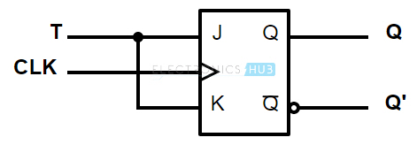
Generally, T flip flops are not available as ICs. So, they can be constructed by using JK flip – flop, SR flip – flop and D flip – flop. The symbol of T flip – flop made from JK flip – flop is shown below.
Applications
Let us now see a couple of important applications of T flip-flop.
- Frequency Division Circuit
- 2 – Bit Parallel Load Registers
Frequency Division Circuit
A T flip–flop can be used as a ‘Frequency Divider Circuit’ by feeding back the complementary output Q’ to the T input. The logic symbol of a frequency divider using T flip – flop is shown below.
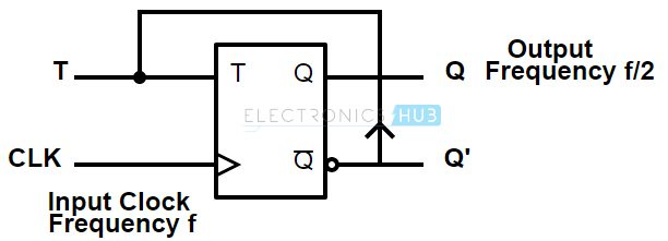 If the input clock frequency of the T flip-flop is ‘f’ Hz, then frequency of the pulse at output Q is ‘f/2’ Hz. We can cascade many such frequency divider circuits to further divide the frequency.
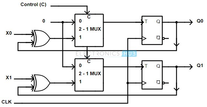
2-Bit Parallel Load Register using T flip – flops
We use registers and shift registers to store the data. But the size is always a primary concern for memory elements such as registers. So, we use 2 – bit parallel load registers instead 4 – bit registers.
There are two operations to be considered when designing a parallel load register:
- Hold the Data
- Parallel Load the Data
To hold the output of T flip – flop, simply the input T should be 0. But the Parallel Load is a difficult part.
Parallel Load means to get the value X at the output of the flip – flop. In order to do that, we XOR the X input and present state output and give it to 2 to 1 MUX. The other input to the MUX is a constant 0 (logic low). The output of the MUX is connected to the input of the T flip – flop.
Since it is a 2–bit register, two such combinations are needed. The circuit of a 2 – bit parallel load register is shown below.
Conclusion
A simple beginner’s tutorial on T Flip-Flop, which is also known as Toggle Flip Flop. You learned how to design a T flip-flop using other flip-flops like SR flip-flop, JK flip-flop and D flip-flop, the working of the Toggle Flip-Flop, truth table of T Flip-Flop and also couple of useful applications.
