In this tutorial, we will learn about SCR Turn ON Methods. There are several SCR Turn On Methods depending various entities like voltage, temperature etc. We will see some of the commonly used methods to turn on SCR.
Outline
ToggleSilicon Controlled Rectifier
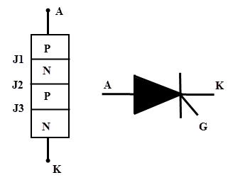
Before looking at the different ways to turn on an SCR i.e., the different SCR turn ON methods, let us quickly recap some important basics of a Silicon Controlled Rectifier or simply known as SCR. An SCR, which is an important member of the Thyristor family, is a semiconductor device with four layers, three junctions and three terminals. The following image shows the structure and symbol of a typical SCR.
SCR is made up of four alternate layers of p-type and n-type semiconductor material. The outer ‘p’ region is connected to the Anode (A) and the outer ‘n’ region is connected to the Cathode (K). The inner ‘p’ region is connected to the third terminal called the Gate (G).
An SCR is essentially a Switch. Unlike Transistor, which can act as a Switch but also as an amplifier, the SCR is only a switch that is either ON or OFF. The SCR has two stable states namely, Forward Blocking State and Forward Conduction State. There are other states but these two are important and hence we will focus only on these two states.
Switching the SCR from forward blocking state (OFF – state) to forward conduction state (ON – state) is known as Turning ON process of SCR. It is also called as triggering.
The criteria for triggering the SCR depends on the several variables like supply voltage, gate current, temperature, etc. There are various methods to trigger the SCR so that it comes into the ON state. Let us discuss some of the SCR Turn On methods in brief.
SCR Turn ON Methods (SCR Triggering)
Let us take the above image with structure of SCR as a reference. If the anode (outer ‘p’ region) is made positive with respect to the cathode (outer ‘n’ region), junctions J1 and J3 become forward biased but the junction J2 becomes reverse biased.
As a result, there is no flow of current through the device except for a small magnitude of leakage current. So, even though the SCR is forward biased, there is still no flow of current and hence, this state is known as Forward Blocking State (OFF State).
NOTE: There is another state known as Reverse Blocking State, where the SCR is reverse biased. The characteristics in this state are similar to that of a regular diode. Let us now focus on bringing the SCR from forward blocking state to forward conduction state by ‘turning on the SCR’.
The SCR can be made to conduct or switched from blocking (non-conducting or OFF) state to Conduction (ON) State by any one of the following methods.
- Forward Voltage Triggering
- Temperature Triggering
- dv/dt Triggering
- Light Triggering
- Gate Triggering
Forward Voltage Triggering
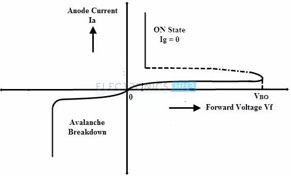
In forward voltage triggering method, the SCR is forward biased i.e., anode is more positive than cathode but this voltage is increased significantly. The gate terminal is kept open.
As the voltage increases, junction J2‘s depletion layer width increases, which in turn increases the accelerating-voltage of minority carriers at this junction. At a particular voltage, there will be an Avalanche Breakdown at the inner junction J2 as a result of minority charge carriers colliding with atoms and releasing even more minority charge carriers.
This voltage is known as Forward Breakover Voltage VBO. At this voltage, the junction J2 becomes forward biased and the SCR turns into conduction state. A large current flows through the SCR (from Anode to Cathode, which is limited by the load resistance) with a very low voltage drop across it.
During the turn ON state, the forward voltage drop across the SCR is in the range of 1 to 1.5 volts and this may be increased with the load current.
In practice this method is not employed because it needs a very large anode to cathode voltage. And also once the voltage is more than the VBO, the SCR turns on and a very high current flows through it instantly, which may cause damage to the SCR. Therefore, most of the cases this type of triggering is avoided.
Temperature Triggering
This type of triggering is also known as Thermal Triggering as the SCR is turned by heating it. The reverse leakage current depends on the temperature. If the temperature is increased to a certain value, the number of hole-pairs also increases. This causes to increase the leakage current and further it increases the current gains of the SCR. This starts the regenerative action inside the SCR since the (α1 + α2) value approaches to unity (as the current gains increases).
By increasing the temperature at junction J2, the width of the depletion layer decreases. So, when the forward bias voltage is near to VBO, we can turn ON the SCR by increasing the junction temperature (J2). At a particular temperature, the reverse bias of the junction breaks down an the device starts to conduct.
This triggering occur in some circumstances particularly when it the device temperature is more (also called false triggering). This type of triggering is practically not employed because it causes the thermal runaway and hence the device or SCR may be damaged.
dv/dt Triggering
In forward blocking state i.e., anode is more positive than cathode, the junctions J1 and J3 are forward biased and the junction J2 is reverse biased. So, the junction J2 behaves as a capacitor (J1 and J3 as conducting plates with a dielectric J2) due to the space charges in the depletion region.
The charging current of the capacitor is given as:
IC = dQ / dt
= d(Cj v) / dt
Using Product Rule of Differentiation, we get
= Cj dv / dt + v dCj / dt
As the junction Capacitance is always almost constant, we can ignore the rate of change of junction Capacitance dCj / dt. So, the final Charging Current is:
IC = Cj dv/ dt
where, IC is the Charging Current
Cj is the Junction Capacitance
Q is the charge
v is the voltage applied across the device
dCj / dt is the rate of change of junction Capacitance
dv / dt is the rate of change of applied voltage
From the above equation, if the rate of change of the applied voltage is large (i.e., it is applied suddenly), then the flow of charging current will increase, which causes the SCR to turn on without any gate voltage.
It is clear that we can turn SCR just by increasing the rate of change of voltage across the device rather than applying a large forward bias voltage (as we did in the previous case). However, this method is also practically avoided because it can cause a false turn ON process and also this can produce very high voltage spikes across the SCR so there will be considerable damage to it.
Light Triggering
An SCR turned ON by light radiation is also called as Light Activated SCR (LASCR). Hence, Light Triggering is also known as Radiation Triggering. Generally, this type of triggering is employed in phase controlled converters in HVDC transmission systems.
In this method, light rays with appropriate wavelength and intensity are allowed to strike the junction J2. The bombarded energy particles from the light (neutrons or photons) causes to break electron bonds as as result, new electron – hole pairs are formed in the device.
As the number of charge carriers are increased, there is an instantaneous increase in the flow of current, causing the SCR to turn ON.
NOTE: For successfully turning ON the SCR with the help of light radiation, the rate of change of applied voltage (dv / dt) must be high.
Gate Triggering
This is most common and most efficient method to turn ON the SCR. When the SCR is forward biased, a sufficient positive voltage at the gate terminal injects some electrons into the junction J2. This results in an increase in the reverse leakage current and hence the breakdown of junction J2 occurs even at a voltage lower than the VBO.
Depending on the size of the SCR, the gate current varies from a few milli-amps to 250 milli-amps or more. If the gate current applied is more, then more electrons are injected into the junction J2 and results to come into the conduction state at much lower applied voltage.
In gate triggering method, a positive voltage applied between the gate and the cathode terminals. We can use three types of gate signals to turn On the SCR. Those are DC signal, AC signal and pulse signal.
DC Gate Triggering
In this triggering, a sufficient DC voltage is applied between the gate and cathode terminals in such a way that the gate is made positive with respect to the cathode. The gate current drives the SCR into conduction mode.
In this method, a continuous gate signal (DC Voltage) is applied at the gate and hence it causes internal power dissipation (or more power loss). Another important drawback is there is no isolation between the power and control circuits (as they both are DC).
AC Triggering
This is the most commonly used method of turning on the SCR, especially in AC applications. With proper isolation between the power and control circuits (using transformers), the SCR is triggered by the phase-shift AC voltage derived from the main supply. The firing angle is controlled by changing the phase angle of the gate signal.
However, only one half of the cycle is available for the gate drive to control the firing angle and for the next half of the cycle, a reverse voltage is applied between the gate and cathode. This is one of the limitation of AC triggering and the other is need for separate step down or pulse transformer to supply the voltage to gate drive from the main supply.
Pulse Triggering
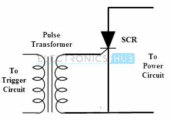
The most popular method of triggering the SCR is the pulse triggering. In this method, gate is supplied with single pulse or a train of high frequency pulses.
The main advantage of this method is that gate drive is discontinuous or doesn’t need continuous pulses to turn the SCR and hence gate losses are reduced in greater amount by applying single or periodically appearing pulses. For isolating the gate drive from the main supply, a pulse transformer is used.
Dynamic Turn ON Switching Characteristics of SCR
The dynamic processes of the SCR are turn ON and turn OFF processes in which both voltage and currents of an SCR vary with time. The transition from one state to another takes finite time, but doesn’t take place instantaneously.
The static or VI characteristics of the SCR give no indication about the speed at which the SCR has switched into forward conduction mode from forward blocking mode. Hence, the dynamic characteristics are sometimes more important which gives the switching characteristics of the SCR.
There will be a finite transition time that SCR takes to reach the forward conduction mode from blocking mode, which is termed as turn ON time (tON) of SCR. The turn ON time of the SCR Ton can be subdivided into three distinct intervals namely delay time td, rise time tr and spread time ts.
Delay Time (td)
The delay time is measured from the instant at which the gate current reaches 90 percent of its final value to the instant at which anode current reaches 10 percent of its final value. It can also be defined as the time taken for the anode voltage to fall from initial anode voltage value Va to 0.9 Va.
Consider the below figure and observe that, until the time td, the SCR is in forward blocking mode, so the anode current is a small leakage current. When the gate signal is applied (at 90 percent of Ig) then the gate current is reached to 0.1 Ia and also correspondingly anode to cathode voltage falls to 0.9 Va.
With the gate signal applied, there will be non-uniform distribution of current over the cathode surface so the current density is much higher at gate terminal. And it rapidly decreases as the distance from gate increases. Hence, the delay time td is the time during which anode current flows in a narrow region where the current density (gate current) is highest.
Rise Time (tr)
This is the time taken by the anode current to rise from 10 percent to 90 percent of its final value. Also defined as the time required for the forward blocking voltage to fall from 0.9 Va to 0.1 Va. This rise time is inversely proportional to the gate current and its rate of building up.
Therefore, if high and steep current pulses are applied at the gate, it can significantly reduce the rise time tr. Also, if the load is inductive, the rise time will be higher and for resistive and capacitive loads it is low.
During this time, turn ON losses in the SCR are high due to large anode current and high anode voltage. This can result in the formation of local hot spots and hence the SCR may be damaged.
Spread Time (ts)
This is the time required for the forward blocking voltage to fall from o.1 Va to its ON-state voltage drop, which is the range of 1 to 1.5 volts. During this time, anode current spread over the entire conducting region of an SCR from a narrow conducting region. After the spreading time, a full anode current flows through the device with small ON-state voltage drop.
Therefore, the total turn ON time tON is:
tON = tr + td + ts
The typical value of the turn ON time is in the order of 1 to 4 micro seconds, depending on the wave shapes of the gate signal and anode circuit parameters. To reduce the turn ON time of the SCR, the amplitude of the gate pulse should be in the order of 3 to 5 times the minimum gate current of the SCR.
SCR Firing Circuits
As we have seen in above that out of various triggering methods to turn the SCR, gate triggering is the most efficient and reliable method. Most of the control applications use this type of triggering because the desired instant of SCR turning is possible with gate triggering method. Let us look on various firing circuits of SCR.
Resistance Firing Circuit
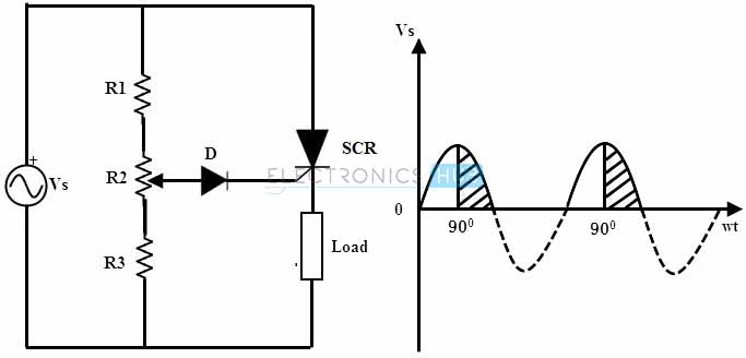
- The circuit below shows the resistance triggering of SCR where it is employed to drive the load from the input AC supply. Resistance and diode combination circuit acts as a gate control circuitry to switch the SCR in the desired condition.
- As the positive voltage applied, the SCR is forward biased and doesn’t conduct until its gate current is more than minimum gate current of the SCR.
- When the gate current is applied by varying the resistance R2 such that the gate current should be more than the minimum value of gate current, the SCR is turned ON. And hence the load current starts flowing through the SCR.
- The SCR remains ON until the anode current is equal to the holding current of the SCR. And it will switch OFF when the voltage applied is zero. So the load current is zero as the SCR acts as open switch.
- The diode protects the gate drive circuit from reverse gate voltage during the negative half cycle of the input. And Resistance R1 limits the current flowing through the gate terminal and its value is such that the gate current should not exceed the maximum gate current.
- It is the simplest and economical type of triggering but limited for few applications due to its disadvantages.
- In this, the triggering angle is limited to 90 degrees only. Because the applied voltage is maximum at 90 degrees so the gate current has to reach minimum gate current value somewhere between zero to 90 degrees.
Resistance – Capacitance (RC) Firing Circuit
- The limitation of resistance firing circuit can be overcome by the RC triggering circuit which provides the firing angle control from 0 to 180 degrees. By changing the phase and amplitude of the gate current, a large variation of firing angle is obtained using this circuit.
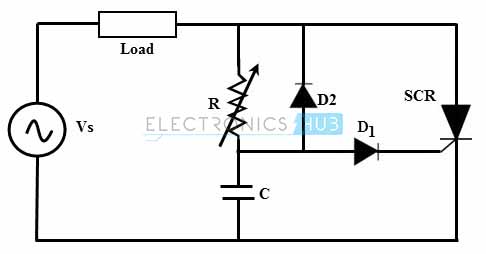
- Below figure shows the RC triggering circuit consisting of two diodes with an RC network connected to turn the SCR.
- By varying the variable resistance, triggering or firing angle is controlled in a full positive half cycle of the input signal.
- During the negative half cycle of the input signal, capacitor charges with lower plate positive through diode D2 up to the maximum supply voltage Vmax. This voltage remains at -Vmax across the capacitor till supply voltage attains zero crossing.
- During the positive half cycle of the input, the SCR becomes forward biased and the capacitor starts charging through variable resistance to the triggering voltage value of the SCR.
- When the capacitor charging voltage is equal to the gate trigger voltage, SCR is turned ON and the capacitor holds a small voltage. Therefore the capacitor voltage is helpful for triggering the SCR even after 90 degrees of the input waveform.
- In this, diode D1 prevents the negative voltage between the gate and cathode during the negative half cycle of the input through diode D2.
UJT Firing Circuit
- It is the most common method of triggering the SCR because the prolonged pulses at the gate using R and RC triggering methods cause more power dissipation at the gate so by using UJT (Uni Junction Transistor) as triggering device the power loss is limited as it produce a train of pulses.
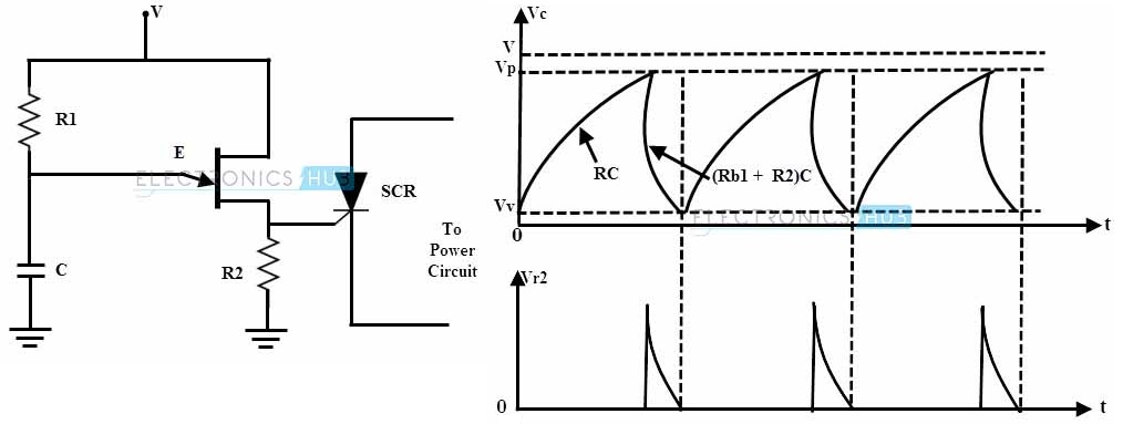
- The RC network is connected to the emitter terminal of the UJT which forms the timing circuit. The capacitor is fixed while the resistance is variable and hence the charging rate of the capacitor depends on the variable resistance means that the controlling of the RC time constant.
- When the voltage is applied, the capacitor starts charging through the variable resistance. By varying the resistance value voltage across the capacitor get varied. Once the capacitor voltage is equal to the peak value of the UJT, it starts conducting and hence produce a pulse output till the voltage across the capacitor equal to the valley voltage Vv of the UJT. This process repeats and produces a train of pulses at base terminal 1.
- The pulse output at the base terminal 1 is used to turn ON the SCR at predetermined time intervals.
Conclusion
A complete tutorial on different types of SCR turn ON Methods. Learn some essential basics of SCR, SCR turn ON Methods like Forward Voltage Triggering, Temperature Triggering, dv/dt Triggering, Light Triggering, Gate Triggering (and its types). Also some of the popular SCR firing circuits.





9 Responses
Good answers, thank you.
Thank you, very nice explanation!
This is exactly what i was looking for, well explained
thnk you sir/ mam very very very very very very very well explained
HOW CAPACITOR WILL CHARGE TO HIGHER VOLTAGE AFTER 90 DEGREE IF AC VOLTAGE IS APPLIED TO IT TO TRIGGER SCR ? ( pl refer RC triggering method of SCR)
How will the IV characteristics sketch look like ? For the following triggering mode of an SCR
_temperature trigger
_Gate trigger
_dv/dt trigger
_light trigger
_forward voltage trigger
I’m so pleased with your explanations. I am now ready to attack my examinations. You’re so amazing. Thanks for the well explained details of SCR.
It was very help full Thanks!
Your explanation is clear