In this tutorial, we will learn about Sample and Hold Circuits. They are a critical part of Analog to Digital Converters and help in accurate conversion of analog signals to digital signals. We will see a simple sample and hold circuit, its working, different types of circuit implementations and some of the important performance parameters.
What is Sample and Hold Circuit?
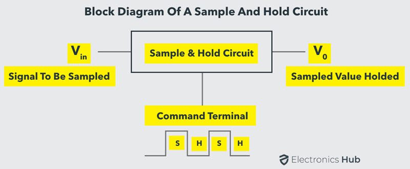
A Sample and Hold Circuit, sometimes represented as S/H Circuit or S & H Circuit, is usually used with an Analog to Digital Converter to sample the input analog signal and hold the sampled signal, hence the name ‘Sample and Hold’.
In the S/H Circuit, the analog signal is sampled for a short interval of time, usually in the range of 10µS to 1µS. After this, the sampled value is hold until the arrival of next input signal to be sampled. The duration for holding the sample will be usually between few milliseconds to few seconds.
The following image shows a simple block diagram of a typical Sample and Hold Circuit.
Need for Sample and Hold Circuits
If the input analog voltage of an ADC changes more than ±1/2 LSB, then there is a severe chance that the output digital value is an error. For the ADC to produce accurate results, the input analog voltage should be held constant for the duration of the conversion.
As the name suggests, a S/H Circuit samples the input analog signal based on a sampling command and holds the output value at its output until the next sampling command is arrived.
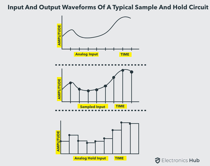
The following image shows the input and output of a typical Sample and Hold Circuit.
Simple Sample and Hold Circuit
Let us understand the operating principle of a S/H Circuit with the help of a simplified circuit diagram. This sample and hold circuit consist of two basic components:
- Analog Switch
- Holding Capacitor
The following image shows the basic S/H Circuit.
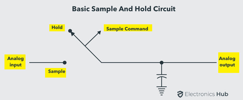
This circuit tracks the input analog signal until the sample command is changed to hold command. After the hold command, the capacitor holds the analog voltage during the analog to digital conversion.
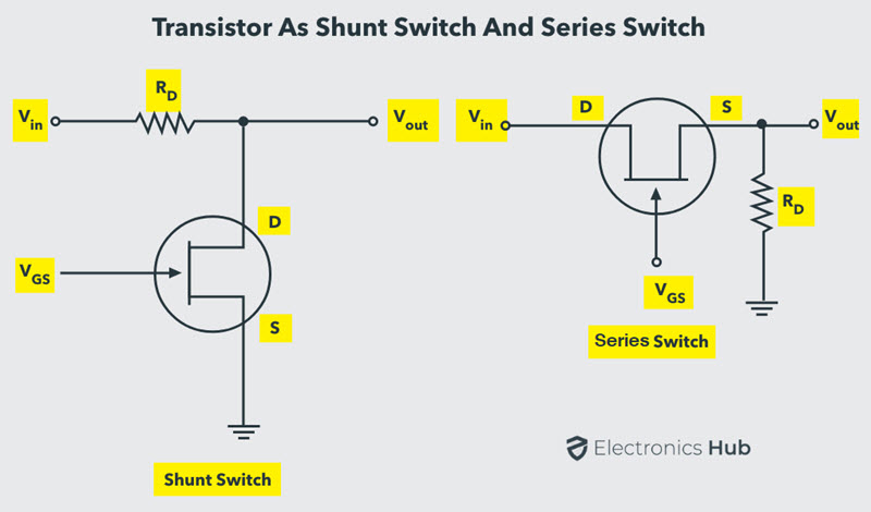
Analog Switch
Any FET like JFET or MOSFET can be used as an Analog Switch. In this discussion, we will concentrate on JFET. The Gate-Source voltage VGS is responsible for switching the JFET.
When VGS is equal to 0V, the JFET acts as a closed switch as it operates in its Ohmic region. When VGS is a large negative voltage (i.e. more negative than VGS(OFF)), the JFET acts as an open switch as it is cut-off.
The switch can be either a Shunt Switch or a Series Switch, depending on its position with respect to input and output. The following image shows a JFET configured as both a Shunt Switch and as a Series Switch.
Types of Sample and Hold Circuits
Let us now see a few different types of Sample and Hold circuits. Note that all the below mentioned circuits use JFET as the switch. During the sampling period, the JFET is turned ON and the charging in the holding capacitor rises to the level of the input analog voltage.
At the end of the sampling period, the JFET is turned OFF and the holding capacitor is isolated from the input signal. This makes sure that the output voltage is held constant at the value of the input voltage irrespective of minor changes in the input value. To compensate for the low drop-out voltage across the holding capacitor, two buffers (voltage followers) are used, one at the input and one at the output.
Keeping this in mind, let us take a look at the first S/H Circuit. The following image shows an open-loop type S/H Circuit.
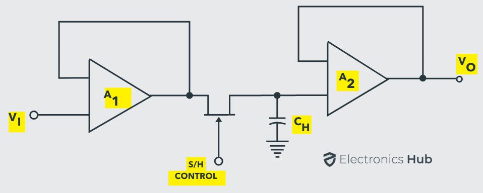
As there is no feedback, this circuit is relatively faster than the coming circuits (which all are in closed-loop configuration). But the feedback in the closed-loop architectures provide higher accuracy figures. The acquisition time (discussed in the next section) must be as low as possible. It is dependent on three factors:
- The RC time constant, where R is the ON Resistance of the JFET (ron) and C is the holding capacitor CH.
- Maximum output current
- Slew-rate of the Op-Amp
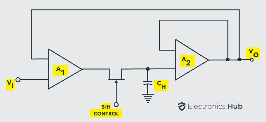
A slightly improved circuit than the first one is presented in the next circuit. In this configuration, the ON Resistance of the JFET is brought into the feedback loop and hence, the acquisition time is dependent on the other two factors.
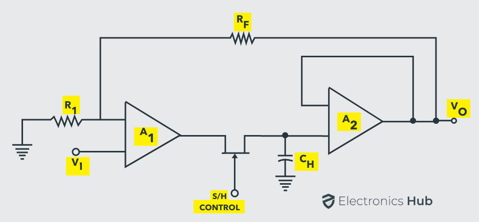
The next circuit is further improved when compared to the previous circuit by providing voltage gain. The voltage gain of the circuit can be calculated using the input resistor R1 and the feedback resistor RF as follows:
A = 1 + (RF / R1)
The final circuit offers additional advantages than the previous circuit. The important one is that the position of the holding capacitor is changed and as a result, the voltage at non-inverting terminal of A2 is equal to the voltage across the capacitor divided by the open-loop gain of A2.
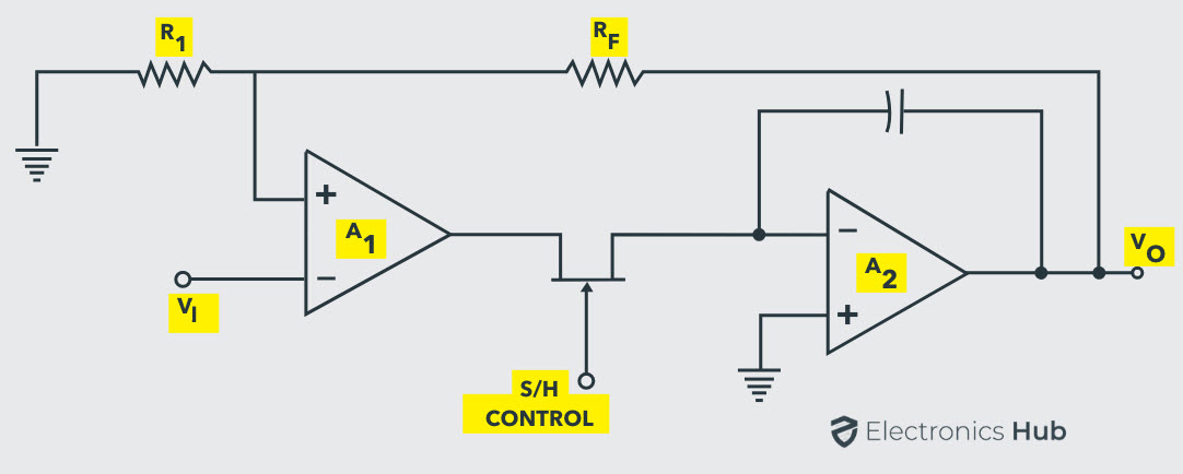
This ensure a faster charging time of the holding capacitor and subsequently a shorter acquisition time.
Performance Parameters
The performance of an S/H Circuit can be characterized by parameters that are commonly used for an amplifier like Input Offset Voltage, Gain Error, Non-linearity and so on. But there are a few characteristics that are specific to the S/H Circuits.
These characteristics are helpful in analyzing its performance during the transition from sampling mode to hold mode (and vice versa) and also during hold mode operations. Let us understand these characteristics with the help of the following image.
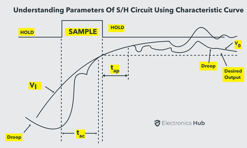
Acquisition Time (tac)
The time required for the charge in the holding capacitor to rise up to a level that is close to the input voltage during the sampling is called acquisition time. It is affected by three factors:
- The RC Time Constant
- The Slew-Rate of the Op-Amp
- The maximum output current of the Op-Amp
Aperture Time (tap)
The time delay between the initiation of Vo tracking the Vi and the initiation of the hold command is called the Aperture Time. This delay is usually due to the propagation delays through the driver and the switch circuits.
For a precise timing operation, the hold command must be initiated in advance by an amount of aperture time.
Aperture Uncertainty (∆ tap)
The Aperture time will not be the same for all the sample and will vary from sample to sample. This uncertainty is called Aperture Uncertainty. This will severely affect the advancing of the hold command.
Hold Mode Settling Time (ts)
The hold mode settling time is the time taken by the output Vo to settle within the specified error band (usually 1%, 0.1% or 0.01%) after the application of hold command.
Hold Step
During the switching from sample mode to hold mode, there might an unwanted transfer of charge between the switch and the holding capacitor (mainly due to the parasitic capacitances). This will affect the capacitor voltage as well as the output voltage. This change in the output voltage from the desired voltage is called Hold Step.
Feedthrough
Again, the parasitic capacitances in the switch may cause AC coupling between Vo and Vi in hold mode. As a result, the output voltage may vary with changes in the input voltage and this is referred to as feedthrough.
Droop
Voltage Droop is a phenomenon where the voltage across the holding capacitor drops down due to leakage currents.
Advantages
- The main and important advantage of a typical SH Circuit is to aid an Analog to Digital Conversion process by holding the sampled analog input voltage.
- In multichannel ADCs, where synchronization between different channels is important, an SH circuit can help by sampling analog signals from all the channels at the same time.
- In multiplexed circuits, the crosstalk can be reduced with an SH circuit.
Applications of Sample and Hold Circuit
Some of the important applications are mentioned below:
- Analog to Digital Converter Circuits (ADC)
- Digital Interface Circuits
- Operational Amplifiers
- Analog De-multiplexers
- Data distribution systems
- Storage of outputs of multiplexers
- Pulse Modulation Systems
Conclusion
A complete beginner’s tutorial on Sample and Hold Circuit. You learned the importance of a sample and hold circuit in Analog to Digital Converters, a simple S/H Circuit using a MOSFET and a Capacitor, different types of Sample and Hold circuits, some important parameters which determine the performance of an S/H circuit and also the applications of S&H Circuits.

One Response
So much helpful for my end sem exam,,, thanks for such a nice article..