Imagine sending HD video, music, emails, phone calls, and internet all down one wire! Multiplexing is the magic trick, and multiplexers (MUX for short) are the tiny wizards behind it. In this guide, learn what is a Multiplexer, different types of multiplexers like 2 to 1, 4 to 1, 8 to 1 and 16 to 1 Multiplexer, commonly available Multiplexer ICs and some important applications of Multiplexers.
What Is Multiplexing?
Multiplexing is the process of combining one or more signals and transmitting on a single channel. In analog communication systems, a communication channel is a scarce quantity, which must be properly used. For cost-effective and efficient use of a channel, the concept of Multiplexing is very useful as it allows multiple users to share a single channel in a logical way.
The three common Types of Multiplexing approaches are:
- Time
- Frequency
- Space
Two of the best examples of Multiplexing Systems used in our day-to-day life are the landline telephone network and the Cable TV.
The device which is responsible for Multiplexing is known as Multiplexer. Multiplexers are used for both Analog and Digital signals. Let us focus on digital signals in this tutorial, to keep things simple. A multiplexer is the most frequently used combinational circuit and it is an important building block in many in digital systems.
These are mostly used to form a selected path between multiple sources and a single destination. A basic multiplexer has various data input lines and a single output line. These are found in many digital system applications such as data selection and data routing, logic function generators, digital counters with multiplexed displays, telephone network, communication systems, waveform generators, etc. In this article we are going to discuss about types of multiplexers and its design.
What Is A Multiplexer?
The multiplexer or MUX is a digital switch, also called as data selector. It is a Combinational Logic Circuit with more than one input line, one output line and more than one select line. It accepts the binary information from several input lines or sources and depending on the set of select lines, a particular input line is routed onto a single output line.
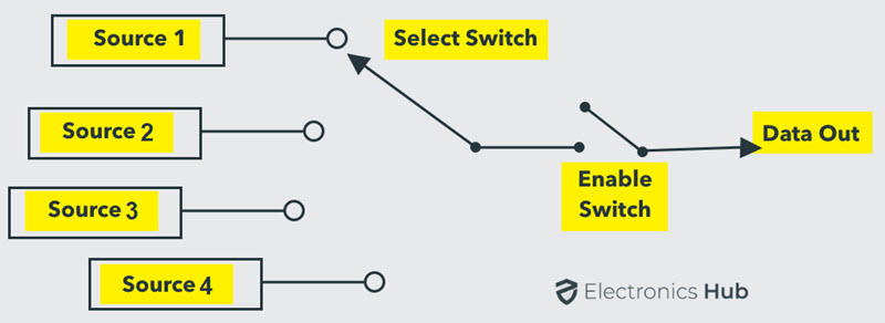
The basic idea of multiplexing is shown in figure below in which data from several sources are routed to the single output line when the enable switch is ON. This is why, multiplexers are also called as ‘many to one’ combinational circuits.
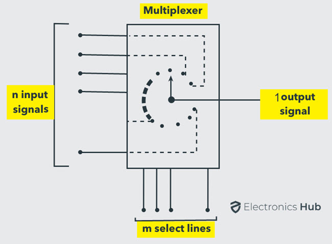
The below figure shows the block diagram of a multiplexer consisting of n input lines, m selection lines and one output line. If there are m selection lines, then the number of possible input lines is 2m. Alternatively, we can say that if the number of input lines is equal to 2m, then m selection lines are required to select one of n (consider 2m = n) input lines.
This type of multiplexer is referred to as 2n × 1 multiplexer or 2n-to-1 multiplexer. For example, if the number of input lines is 4, then two select lines are required. Similarly, to select one of 8 input lines, three select lines are required.
Generally, the number of data inputs to a multiplexer is a power of two such as 2, 4, 8, 16, etc. Some of the most frequently used multiplexers include 2-to-1, 4-to-1, 8-to-1 and 16-to-1 multiplexers.
These multiplexers are available in IC forms with different input and select line configurations. Some of the available multiplexer ICs include 74157 (Quad 2-to-1 MUX), 78158 (Quad 2-to-1 MUX with inverse output), 74153 (4-to-1 MUX), 74152 (8-to-1 MUX) and 74150 (16-to-1 MUX).
Also Read: What Is A Demultiplexer
2 to1 Multiplexer
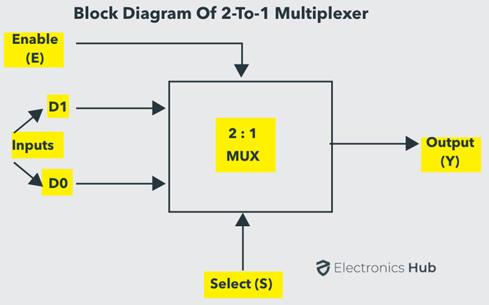
A 2 to 1 multiplexer consists of two inputs D0 and D1, one select input S and one output Y. Depending on the select signal, the output is connected to either of the inputs. Since there are two input signals, only two ways are possible to connect the inputs to the outputs, so one select is needed to do these operations.
If the select line is low, then the output will be switched to D0 input, whereas if select line is high, then the output will be switched to D1 input. The figure below shows the block diagram of a 2:1 mux which connects two 1-bit inputs to a common destination.
2×1 Multiplexer Calculator
2×1 multiplexer truth table is shown below. Depending on the value of the select input, the inputs i.e., D0, D1 are produced at outputs. The output is D0 when Select value is S = 0 and the output is D1 when Select value is S = 1.
| S | D0 | D1 | Y |
| 0 | 0 | X | 0 |
| 0 | 1 | X | 1 |
| 1 | X | 0 | 0 |
| 1 | X | 1 | 1 |
‘X’ in the above 2:1 multiplexer truth table denotes a don’t care condition. So, ignoring the don’t care conditions, we can derive the MUX Boolean Expression of a typical 2:1 Multiplexer as follows:
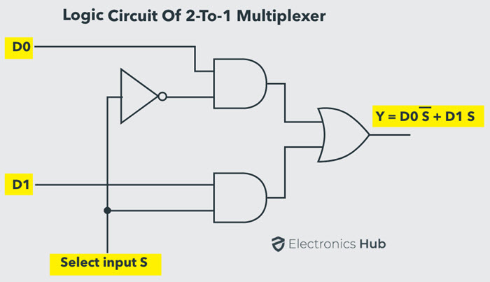
Y = SD0 + SD1
From the above output expression, the logic circuit of 2-to-1 multiplexer can be implemented using logic gates as shown in figure. It consists of two AND gates, one NOT gate and one OR gate. When the select line, S=0, the output of the lower AND gate is zero, but the output of upper AND gate is D0. Thus, the output generated by the OR gate is equal to D0.
Similarly, when S=1, the output of the upper AND gate is zero, but the output of lower AND gate is D1. Therefore, the output of the OR gate is D1. Thus, the above given mux Boolean expression is satisfied by this circuit.
In order to efficiently use the Silicon, IC Manufacturers fabricate multiple Multiplexers in a single IC. Generally four 2 line to 1 line multiplexers are fabricated in a single IC. Some of the popular ICs of 2 to 1 multiplexers include IC 74157 and IC 74158.
Both these ICs are Quad 2-to-1 Multiplexers. While IC 74157 has a normal output, the IC74158 has an inverted output. There is only one selection line, which controls the input lines to the output in all four multiplexers.
The output Y0 can be either A0 or B0 depending on the status of the select line. Similarly, Y1 can be either A1 or B1, Y2 can be either A2 or B2 and so on. There is an additional Strobe or Enable control input E/Strobe, which enables and disables all the multiplexers, i.e., when E=1, outputs of all the multiplexer is zero irrespective of the value of S.
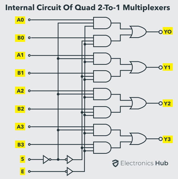
All the multiplexers are activated only when the E / Strobe input is LOW.
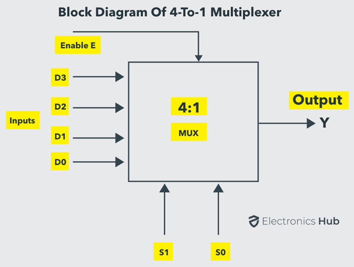
4 to 1 Multiplexer
A 4 to 1 multiplexer consists four data input lines as D0 to D3, two select lines as S0 and S1 and a single output line Y. The select lines S0 and S1 select one of the four input lines to connect the output line. The figure below shows the block diagram of a 4:1 multiplexer in which, the multiplexer decodes the input through select line.
4×1 Multiplexer Calculator
The 4×1 multiplexer truth table is shown below in which four input combinations 00, 10, 01 and 11 on the select lines respectively switches the inputs D0, D2, D1 and D3 to the output. That means when S0=0 and S1 =0, the output at Y is D0, similarly Y is D1 if the select inputs S0=0 and S1= 1 and so on.
| S0 | S1 | D0 | D1 | D2 | D3 | Y |
| 0 | 0 | 0 | X | X | X | 0 |
| 0 | 0 | 1 | X | X | X | 1 |
| 0 | 1 | X | 0 | X | X | 0 |
| 0 | 1 | X | 1 | X | X | 1 |
| 1 | 0 | X | X | 0 | X | 0 |
| 1 | 0 | X | X | 1 | X | 1 |
| 1 | 1 | X | X | X | 0 | 0 |
| 1 | 1 | X | X | X | 1 | 1 |
From the above 4:1 multiplexer truth table, we can write the output expressions as follows:
Y = S0 S1 D0 + S0 S1 D1 + S0 S1 D2 + S0 S1 D3
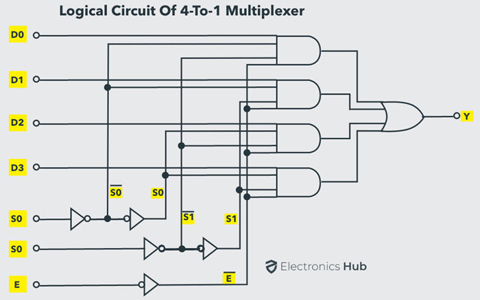
From the above expression of the output, a 4-to-1 multiplexer can be implemented by using basic logic gates. The below figure shows the logic circuit of 4:1 MUX which is implemented by four 3-inputs AND gates, two 1-input NOT gates, and one 4-inputs OR gate.
In this circuit, each data input line is connected as input to an AND gate and two select lines are connected as other two inputs to it. Additionally, there is also an Enable Signal. The output of all the AND gates are connected to inputs of OR gate in order to produce the output Y.
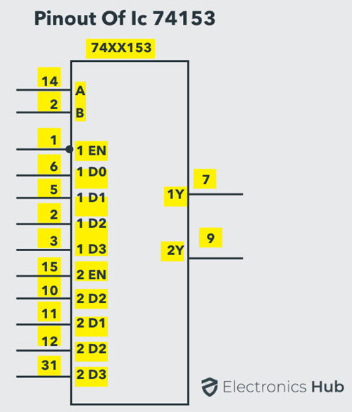
Generally, this type of multiplexers is available in IC with dual mode i.e., there will be two 4-to-1 Multiplexers in a single IC. The most common and popular 4-to-1 line multiplexer is IC 74153 which, is a dual 4-to-1 line multiplexer. It consists of two identical 4-to-1 multiplexers. It has two separate enable or strobe inputs to switch ON or OFF the individual multiplexers. But the Select lines are common to both the Multiplexers.
Usually, the enable input or strobe can be used to cascade two or more multiplexer ICs to construct a multiplexer with large number of inputs. Each multiplier is supplied with separate inputs. The figure below shows the pin diagram of IC74153.
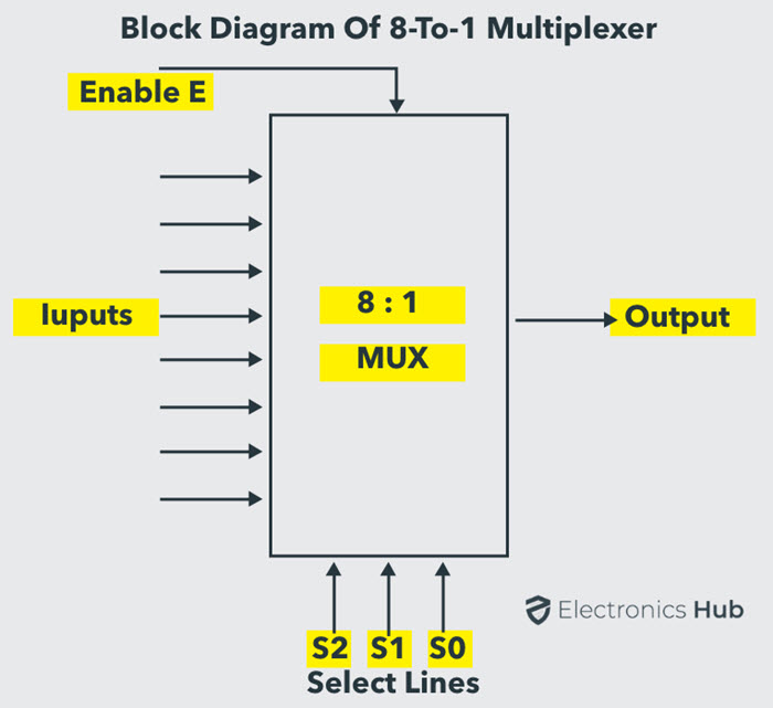
8 to 1 Multiplexer
An 8 to 1 multiplexer consists of eight data inputs D0 through D7, three input select lines S0 through S2 and a single output line Y. Depending on the select lines combinations, multiplexer selects the inputs.
The below figure shows the block diagram of an 8-to-1 multiplexer with enable input that can enable or disable the multiplexer. Since the number data bits given to the MUX are eight, then 3 bits (23 = 8) are needed to select one of the eight data bits.
8×1 Multiplexer Calculator
The 8 to 1 multiplexer truth table is given below with eight combinations of inputs so as to generate each output corresponds to input.
For example, if S2= 0, S1=1 and S0=0 then the data output Y is equal to D2. Similarly the data outputs D0 to D7 will be selected through the combinations of S2, S1 and S0 as shown in below figure.
| S0 | S1 | S2 | D0 | D1 | D2 | D3 | D4 | D5 | D6 | D7 | Y |
| 0 | 0 | 0 | 0 | X | X | X | X | X | X | X | 0 |
| 0 | 0 | 0 | 1 | X | X | X | X | X | X | X | 1 |
| 0 | 0 | 1 | X | 0 | X | X | X | X | X | X | 0 |
| 0 | 0 | 1 | X | 1 | X | X | X | X | X | X | 1 |
| 0 | 1 | 0 | X | X | 0 | X | X | X | X | X | 0 |
| 0 | 1 | 0 | X | X | 1 | X | X | X | X | X | 1 |
| 0 | 1 | 1 | X | X | X | 0 | X | X | X | X | 0 |
| 0 | 1 | 1 | X | X | X | 1 | X | X | X | X | 1 |
| 1 | 0 | 0 | X | X | X | X | 0 | X | X | X | 0 |
| 1 | 0 | 0 | X | X | X | X | 1 | X | X | X | 1 |
| 1 | 0 | 1 | X | X | X | X | X | 0 | X | X | 0 |
| 1 | 0 | 1 | X | X | X | X | X | 1 | X | X | 1 |
| 1 | 1 | 0 | X | X | X | X | X | X | 0 | X | 0 |
| 1 | 1 | 0 | X | X | X | X | X | X | 1 | X | 1 |
| 1 | 1 | 1 | X | X | X | X | X | X | X | 0 | 0 |
| 1 | 1 | 1 | X | X | X | X | X | X | X | 1 | 1 |
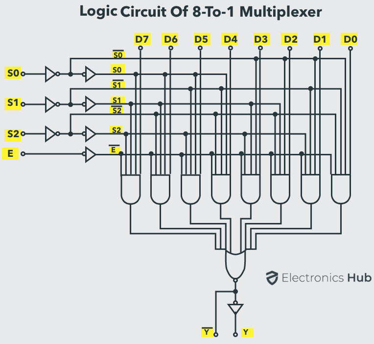
From the above 8:1 multiplexer truth table, the Boolean equation for the output is given as:
Y = S0 S1 S2 D0 + S0 S1 S2 D1 + S0 S1 S2 D2 + S0 S1 S2 D3 + S0 S1 S2 D4 + S0 S1 S2 D5 + S0 S1 S2 D6 + S0 S1 S2 D7
From the above Boolean equation, the logic circuit diagram of an 8-to-1 multiplexer can be implemented by using 8 AND gates, 1 OR gate and 7 NOT gates as shown in below figure. In the circuit, when enable pin is set to one, the multiplexer will be disabled and if it is zero, then select lines will select the corresponding data input to pass through the output.
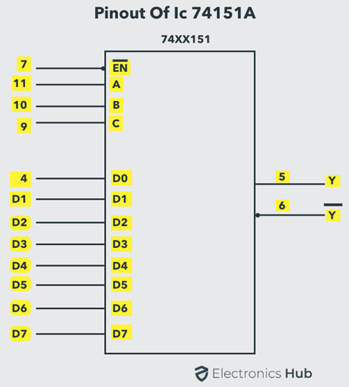
IC 74151 is a popular 8-to-1 multiplexer IC with eight inputs and two outputs. The two outputs are active low and active high outputs. It has three select lines A, B and C and one active low enable input. The pinout of this IC is given below.
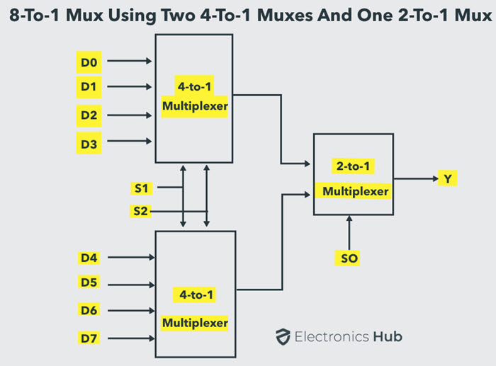
8 to 1 Mux Using 4 to 1 Mux And 2 to 1 Mux
If you observe the Boolean Expression of 8-to-1 Multiplexer shown above, we can re-write it as follows:
Y = S0 S1 S2 D0 + S0 S1 S2 D1 + S0 S1 S2 D2 + S0 S1 S2 D3 + S0 S1 S2 D4 + S0 S1 S2 D5 + S0 S1 S2 D6 + S0 S1 S2 D7
Y = S0 (S1 S2 D0 + S1 S2 D1 + S1 S2 D2 + S1 S2 D3) + S0( S1 S2 D4 + S1 S2 D5 + S1 S2 D6 + S1 S2 D7)
The expression in the first bracket i.e., S1 S2 D0 + S1 S2 D1 + S1 S2 D2 + S1 S2 D3 is similar to the multiplexer Boolean Expression of a 4-to-1 Multiplexer with D0, D1, D2 and D3 as inputs and S1 and S2 as Select Lines. Let this expression be P1.
Similarly, the expression in the second bracket i.e., S1 S2 D4 + S1 S2 D5 + S1 S2 D6 + S1 S2 D7 is similar to the multiplexer Boolean Expression of another 4-to-1 Multiplexer with D4, D5, D6 and D7 as inputs and S1 and S2 as Select Lines. Let this expression be P2.
Now, replacing the above expressions with P1 and P2, we get,
S0 P1 + S0 P2
This expression is similar to a 2-to-1 Multiplexer with P1 and P2 (where, P1 and P2 are outputs of respective 4-to-1 Multiplexers) as Inputs and S0 as Select Signal. So, finally, we can deduce that an 8-to-1 Multiplexer can be implemented using two 4-to-1 Multiplexers and one 2-to-1 Multiplexer. The block diagram of the same is shown below:
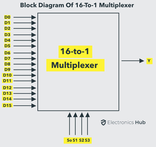
16 to 1 Multiplexer
All the higher order Multiplexers like 8-to-1, 16-to-1, etc. can be implemented using lower order multiplexers. But none the less, let us take a quick look at 16-to-1 Multiplexer. IC 74150 is a popular 16-to-1 Multiplexer IC. The inputs to a 16:1 MUX are D0, D1, D2 and so on up tp D15. Since it has 16 input lines, there will be 4 select lines namely S0, S1, S2 and S3.
The following image shows the block diagram of a typical 16 to 1 Multiplexer.
Simplified truth table for 16×1 Multiplexer is shown in the following table.
| S0 | S1 | S2 | S3 | Y |
| 0 | 0 | 0 | 0 | D0 |
| 0 | 0 | 0 | 1 | D1 |
| 0 | 0 | 1 | 0 | D2 |
| 0 | 0 | 1 | 1 | D3 |
| 0 | 1 | 0 | 0 | D4 |
| 0 | 1 | 0 | 1 | D5 |
| 0 | 1 | 1 | 0 | D6 |
| 0 | 1 | 1 | 1 | D7 |
| 1 | 0 | 0 | 0 | D8 |
| 1 | 0 | 0 | 1 | D9 |
| 1 | 0 | 1 | 0 | D10 |
| 1 | 0 | 1 | 1 | D11 |
| 1 | 1 | 0 | 0 | D12 |
| 1 | 1 | 0 | 1 | D13 |
| 1 | 1 | 1 | 0 | D14 |
| 1 | 1 | 1 | 1 | D15 |
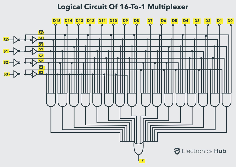
The Boolean Expression of a 16-to-1 Multiplexer is as follows:
Y = S0 S1 S2 S3 D0 + S0 S1 S2 S3 D1 + S0 S1 S2 S3 D2 + S0 S1 S2 S3 D3 + S0 S1 S2 S3 D4 + S0 S1 S2 S3 D5 + S0 S1 S2 S3 D6 + S0 S1 S2 S3 D7 + S0 S1 S2 S3 D8 + S0 S1 S2 S3 D9 + S0 S1 S2 S3 D10 + S0 S1 S2 S3 D11 + S0 S1 S2 S3 D12 + S0 S1 S2 S3 D13 + S0 S1 S2 S3 D14 + S0 S1 S2 S3 D15
The following image shows the logical circuit of a 16-to-1 Multiplexer.
Similar to an 8-to-1 Multiplexer, we can implement 16-to-1 Multiplexer using lower order multiplexers like 8-to-1, 4-to-1 and 2-to-1. The following image shows the block diagram of a 16-to-1 Multiplexer implemented using two 8-to-1 Multiplexers and one 2-to-1 Multiplexer.
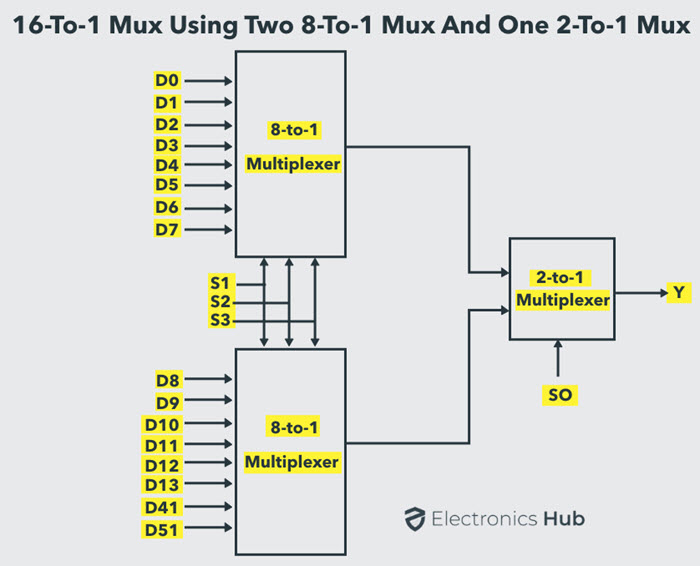
Further, we can implement the individual 8-to-1 Multiplexers in the above image using two 4-to-1 Multiplexers and one 2-to-1 Multiplexer.
Application of Multiplexer
In all types of digital system applications, multiplexers find its immense usage. Since these allows multiple inputs to be connected independently to a single output, multiplexers are found in variety of applications including data routing, logic function generators, control sequencers, parallel-to-serial converters, etc.
Multiplexers are used in telecommunications for data routing, in computer memory to select data lines, in broadcasting to combine multiple audio or video signals, and in various electronic devices for signal processing.
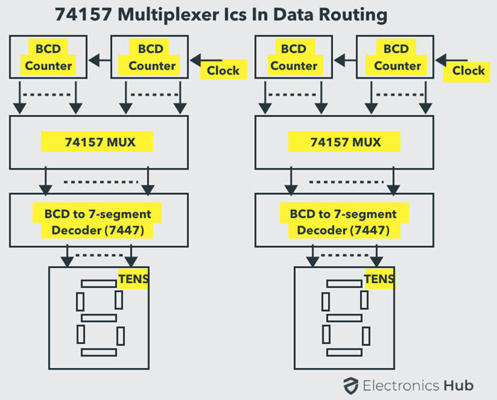
Data Routing
Multiplexers are extensively used in data routing applications to route the data to a one particular destination from one of several sources. One of the applications includes the displaying of two multidigit BCD counters, one at a time. In such application, 74157 multiplexer ICs are used to select and display the content of either of two BCD counters using a set of decoder and LED displays.
Logic Function Generator
In place of logic gates, a logical expression can be generated by using a multiplexer. It is possible to connect the multiplexer such that it duplicates the logic of any truth table. In such cases it can generate the Boolean algebraic function of a set of input variables.
This abruptly reduces the number of logic gates or integrated circuits to perform the logic function since the multiplexer is a single integrated circuit. In this kind of applications, multiplexers are viewed as logic function generators.
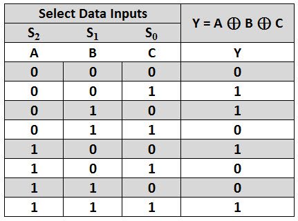
For example consider the below logic diagram to implement the ex-OR function of three inputs. A 74151A 8-to-1 multiplexer is used in this logic generator. This multiplexer works exactly similar to the set of logic gates implementing the same function.
The output F is 1 for data inputs D1, D2, D5 and D6 which are selected by making selection lines to 001, 010, 100 and 111 respectively.
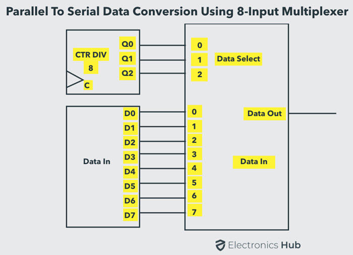
Parallel to Serial Conversion
A multiplexer circuit can be used to convert the parallel data to serial data in order to reduce the number of parallel buses by converting them to serial signals. This type of conversion is needed in telecommunication, test and measurement, military/aerospace, data communications applications.
Mostly in digital systems, data is processed in parallel for achieving higher speeds. But for transmission of the data signals over long distances, we need more number of lines. In such cases, parallel data is converted into serial form using multiplexers.
The figure below shows the parallel to serial data conversion using an 8 input multiplexer. Parallel data from the data in or some other register is applied to the 8 input lines of the multiplexer.
The selection codes for the multiplexer are generated by a 3-bit counter. With the application of each clock pulse to the counter the data is serially out from the multiplexer.
Other applications of multiplexers include control sequencers, pulse train generators, encoders, register to register data transfer, waveform generators, etc.
Conclusion
Complete tutorial on Multiplexer (MUX) and Multiplexing. You learned the basics of Multiplexing, multiplexer, different types of commonly used multiplexers like 2:1 MUX, 4:1 MUX, 8:1 MUX and 16:1 MUX, their multiplexer Boolean Expressions, logic circuits and also couple of important applications of Multiplexers.
FAQs: Multiplexers And Multiplexing
How does a multiplexer differ from a demultiplexer?
A multiplexer (MUX) combines multiple input signals into one output signal, while a demultiplexer (DEMUX) takes a single input signal and routes it to one of several outputs.
What are the key factors to consider when selecting a multiplexer for a project?
Key factors include the number of input channels, signal type (analog or digital), speed requirements, power consumption, and compatibility with the rest of the system.
How does a multiplexer improve the efficiency of data transmission?
A multiplexer allows multiple signals to be transmitted over a single channel, reducing the need for multiple communication lines and improving bandwidth efficiency.
How do multiplexers affect signal integrity?
Multiplexers can introduce signal degradation due to factors like crosstalk, noise, and propagation delay. Proper design and shielding can mitigate these effects.
Are there software-based multiplexers?
Yes, software-based multiplexers exist and are used in applications like operating systems and networking software to manage multiple data streams and virtual channels.

17 Responses
can u explain 16 to 1 multiplexer
Yes. 16 to 1 multiplexer is a 16 to 1 multiplexer.
The content is good
Thanks for giving us such kind of imp. Information
It’s helpful
how to implement mux into full adder / full subtractor and half adder/ half subtractor.
Can u explain 6-1 multiplexer
Can you please explain 3×4 multiplexer
can u plzz explain 16:1 multiplexer
Can u add 10×1 plizz
good
thanx for this information..very helpful content and easy to understand
thank you for this info.and very helpful content easy to understand
very helpful content easy to understand
Great explanation! Finally i understand this logic gate in depth.
it is simple and understandable easily. it’s giving more information. thank you
Excellent article.
Caught a little error. The logical circuit of a 4-to-1 MUX represents the S1 line as S0.