In this tutorial, we will have a brief introduction to Logic Gates. We will see the different Logic Levels in TTL Circuits, CMOS Circuits, some simple Logic Gates like OR, NOT, NAND, AND, etc.
Introduction to Logic Gates
Logic gates are the heart of digital electronics. A gate is an electronic device which is used to compute a function on a two valued signal. Logic gates are the basic building block of digital circuits.
Basically, all logic gates have one output and two inputs. Some logic gates like NOT gate or Inverter has only one input and one output. The inputs of the logic gates are designed to receive only binary data (only low 0 or high 1) by receiving the voltage input.
The low logic level represents Zero volts and high logic level represents 3 or 5 volts positive supply voltage.
We can connect any number of logic gates to design a required digital circuit. Practically, we implement the large number of logic gates in ICs, by which we can save the physical space occupied by the large number of logic gates. We can also perform complicated operations at high speeds by using integrated circuits (IC).
By combining logic gates, we can design many specific circuits like flip flops, latches, multiplexers, shift registers etc.
Digital logic levels
A logic level is defined as a specific state or voltage of a signal. We know that 0 and 1 are the two states of logic gates. The logic levels 0 and 1 are known as LOW and HIGH respectively. In digital electronics, these binary logic levels play a crucial role in data storage, data transfer.
Generally these logic levels can be understand as ON and OFF states. As we said earlier, the logic levels are introduced to the logic gate by the supply voltage. If the supply voltage to the logic gate is 0 volts, it refers to Low logic level or OFF state.
Similarly, if the supply voltage to the logic gate is 5 volts or 3.3 volts (for modern ICs), it refers to High logic level or ON state. The manufacturers will follow the TTL or Transistor – Transistor Logic as standard voltage level, while designing the ICs.
What is Active High and Active Low?
We see the active high input and active low input pins in ICs and micro controllers. Do you know what they really mean? They just describe us how the pin is getting activated.
This means the Active low pin must be connected to low logic level or Ground. In the same way, the Active high pin must be connected to high logic level or to 5 volts or 3.3 Volts.
Let’s understand about this in a simple way. When we see the enable pin CE in a shift register IC, without any line (bar) on it, we connect it to active low input i.e. to ground 0 volts. Otherwise, if we see the enable pin with a line on it as (CE) ̅, we connect it to the active high input i.e. to 3.3 or 5 volts supply, in order to enable the pin.
TTL Logic Levels
TTL logic level is the standard logic level for majority of the logic devices. TTL means Transistor – Transistor Logic. Transistors are electrically controlled switches. The voltage levels of logic families are
VOH – min. output voltage level for HIGH signal
VOL – max. Output voltage level for LOW signal
VIH – min. input voltage level of a device to be considered for HIGH signal
VIL – max. Input voltage level of a device to be considered for LOW signal
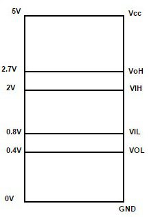
If we observe the TTL logic levels, we can observe that the minimum high voltage level for output is 2.7 volts. This means, when the device is driving HIGH, the voltage should be at least 2.7 volts.
Similarly, the minimum high voltage level for input is 2 volts. So the voltages greater than 2 volts will considered as logic 1, to a TTL device. The voltages between 0.8 volts and 2 volts are known as noise margin.
In the same way, the maximum LOW voltage level for output is 0.4 volts. This means, when the device is driving HIGH, the voltage should be less than 0.4 volts. Similarly, the maximum low voltage level for input is 0.8 volts.
So the voltages less than 0 volts will consider as logic 0, to a TTL device. So when the logic device is supplied with voltages between 0.8 V and 2 V, then logic level of the device will change between High and Low. This situation is called ‘Floating’.
Another procedure for input and output tolerances of TTL device is
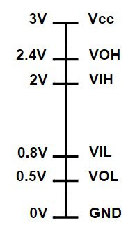
CMOS Logic Levels
CMOS logic devices are also known as 3.3 volt devices, because the CMOS devices will have the maximum voltage level as 3.3 V. This is an advanced technology that will run the devices on low power supply (3.3 V instead of 5 V).
Mostly we use 5V devices (TTL compatible) to design logic gates, so these CMOS devices are used to interface with TTL devices. A CMOS device can interface with any TTL device and they do not require any additional components.
For example, the minimum value for a high logic level (1) of a CMOS device is 2.4 V. So this device can be interpreted with TTL device which has minimum input voltage for logic (V¬IH) 1 as 2 V.
But, before interfacing the TTL to CMOS devices (3.3 V and 5 V) we need to check that the 3.3 V devices are 5 V tolerant or not. Because many of the will permanently cause the chip damage when we supply voltages above 3.6 V. We can use a voltage divider circuit or logic level shifters to control the 5 V voltage signals.
Noise Margin
The noise margin of a logic level is defined as the voltage gap between the maximum low voltage of high input (VIL max) and maximum voltage of the low input (VIL min) of a logic gate. The noise margin is also defined as the amount by which the voltage signal exceeds the threshold level for the exact high or exact low.
Let’s clearly understand this with an example. When a logic circuit is altering between 0 volts and 1.2 volts, with any voltage below 0.2 volts is considered as LOW i.e. 0. And any voltage above 1 volt is considered as HIGH i.e. 1.
CMOS logic devices have higher noise level or noise margin than TTL logic devices because their minimum output voltage for high logic (VOH min) is closer to the supply voltage and maximum output voltage for low logic (VOL max) is nearly 0. So the noise level is the maximum amount of noise that a logic circuit can withstand.
If we apply a voltage of certain the noise level, we do not certainly know whether the circuit will respond or not. Noise level is the unwanted voltage level, caused by external interference such as supply voltage fluctuations and other conductors in circuit.
The noise level that a circuit can tolerate is called as “Noise immunity” or “Noise margin”. For TTL devices the tolerance range of output voltages is higher than that of input voltages.
Simple Diode Logic Gates
Diodes can act like switches, so these are used in digital logic operations and switching. For low and high impedance states a diode will work in forward bias and reverse bias.
The diode will conduct only in one direction (Forward bias) and it remains closed in reverse bias condition. So it behaves like a switch. Now let’s see some simple diode logic gates, which are constructed by using only Diodes and resistors.
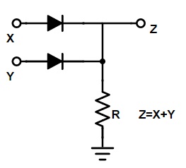
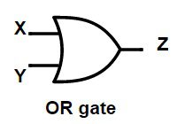
OR Gate
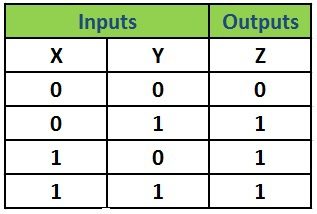
The simple OR gate designed by two diodes is shown in the below figure. Inputs are given to this circuit by the two diodes. In this, the logic HIGH (1) is represented by +5 Volts and logic LOW (0) is represented by 0 Volts or Ground.
In the circuit below, the two inputs are left unconnected, so the output is 0 i.e. logic low.
If any one of the two inputs is connected to +5 volts, then the diode becomes forward biased and it will conduct .Thus the output is logic HIGH i.e. 1.
If voltage of +5 V is connected to both the inputs (both diodes), they will be in forward biased state, which makes the output of OR circuit to set in HIGH logic.
The functioning of OR gate is mathematically given as Z = X + Y, where Z is the output of the OR gate and X, Y are the inputs. The truth table and logic diagram and circuit diagram for the logical OR gate is shown below.
AND Gate
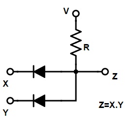
The simple AND gate designed by two diodes is shown in the below figure. In this the circuit driving voltage V is connected to the two parallelly connected diodes through a resistor, R. Inputs are given to this circuit by the two diodes.
In this, the logic HIGH (1) is represented by +5 Volts and logic LOW (0) is represented by 0 Volts or Ground.
In the below circuit , the two inputs are left unconnected, so the output is also 0 i.e. logic low.
If any one of the two inputs is connected to +0 volts , then the diode becomes reverse biased and it will not conduct and makes the output as LOW logic i.e. 0.
If the voltage of +5 V is connected to both the inputs (both diodes) , both the diodes will be in forward biased state, which makes the output of AND circuit to set in HIGH logic.
The functioning of AND gate is mathematically given as Z = X. Y, where Z is the output of the AND gate and X, Y are the inputs. The truth table and logic diagram and circuit diagram for the logical AND gate is shown below.
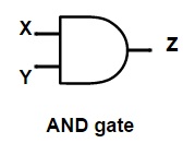

AND logic circuit Logic symbol Truth table
Transistor Logic Gates
Like diode, transistor also acts as an electronic switch. We can design logic gates using transistors also. Let’s have a look about the transistor -made logic gates.
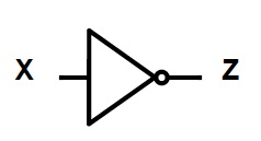
NOT Gate
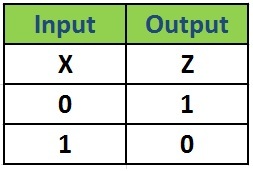
The NOT gate is generally known as an INVERTER. It produces the exact reverse output to that of given input. It has only one input and one output. The output of NOT gate is always the complement of its input. When low input signal is connected to the input of the NOT gate, then the output will be HIGH (logic 1).
Similarly, if high input signal is connected to the input, then the output will be LOW (logic 0). The NOT operation is denoted by ‘-’ bar symbol. If the input of NOT gate is X and output is Z then the operation of NOT gate is given as Z =X ̅, said as X bar.
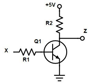
The NOT gate designed by using transistor is shown below. The input is given to the base of the transistor through a resistor. And this transistor circuit is driven by a +5 volts voltage.
When the input is connected to low level signal 0 V, then the transistor will be reverse biased. So no current will flow through it, thus it remains in OFF. As there is no current flow through transistor, there will be no voltage drop across the resistor. So the output will correspond to +5 Volts making the output logic HIGH.
But if +5 V connected to the input, the output voltage will become 0. The transistor designed NOT gate is shown below.
There are two more gates which can be designed by using transistors, they are NAND gate and NOR gate. These gates are called “Universal gates”.
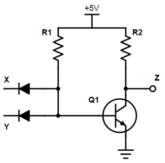
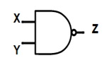
NAND Gate
The NAND gate has the ability to perform 3 operations such as AND, OR and NOT. This gate is a combination of NOT & AND gates. The NAND gate output is equal to the inverse of the AND gate.
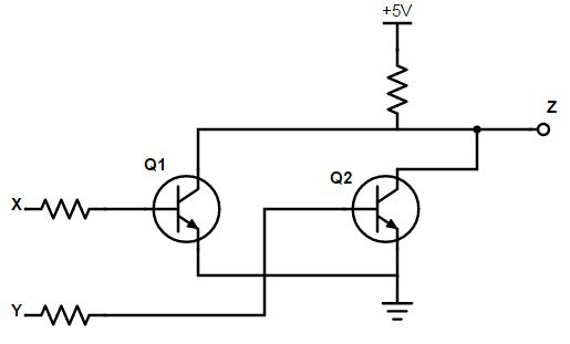
The NAND gate has two inputs X and Y, and a single output Z. The inputs are applied to the diodes which are connected to the transistor. The NAND gate circuit is driven by +5 Volts.
When both inputs are connected to a voltage supply of 5 V, then both diodes D1 and D2 are in OFF state. Then the transistor Q1 is able to drive from the supply voltage through the resistor. So the transistor is in ON state and the output voltage Vce (Sat) becomes 0.
Similarly, when low level voltage is applied the to the inputs i.e. 0 V, the transistor will be OFF and the output voltage becomes +5 V. Mathematically NAND gate is represented as Z =(X.Y) ̅.
So the output of the NAND gate becomes LOW only when both the inputs are high. It becomes HIGH for any other combination of inputs. The truth table, logic symbol and transistor circuit diagrams of NAND gate are shown below.

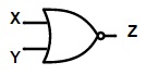
NOR Gate
NOR gate is the combination of NOT gate and OR gate. The NOR gate output is equal to the inverse of the OR gate. The NOR gate has two inputs X and Y, and a single output Z.
The transistor designed NOR gate has two n-p-n transistors in it with the voltage supply or +5 Volts.
When both the inputs of the NOR gate are connected to 0 Volts, then the transistors Q1 and Q2 are in OFF state. So no current flows through the resistor and there is no voltage drop across the resistor. Then the output voltage is equal to the supply voltage +5 Volts i.e. HIGH logic level.
If any one of the input is connected to +5 V, then the transistors will be ON state. So the voltage drop would be high. So the output voltage of the circuit will be 0 V i.e. equal to ground voltage.
Mathematically NOR gate is represented as Z =(X+Y) ̅.
So the output of the NAND gate becomes HIGH only when both the inputs are low. It becomes LOW for any other combination of inputs. The truth table, logic symbol and transistor circuit diagrams of NOR gate are shown below.

74 Series Logic IC’s
The 7400 series ICs are introduced in and around 1960s. Though many other ICs for logic gates are in use, the 7400 TTL family ICs have become most popular because of their simple numbering scheme and standards. Some of the specifications and main features are given below.
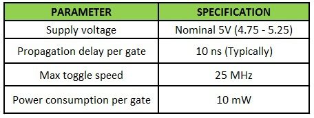
The 74 series ICs are fabricated by using bipolar transistor technology, so they are named as TTL family ICs. (TTL means Transistor -Transistor Logic). The 7400 ICs will work on the supply of +5 volts and this became the standard voltage level of logic circuits for many years, till the evolution of CMOS technology.
These are the widely used IC series for logic circuit design. Earlier to this 7400 series ICs, we have TTL series chips. Motorola Company launched a logic family with the name MTTL, which means Motorola Transistor -Transistor Logic.
Other researchers and manufacturers like, Signetics, Fairchild and National Semiconductor are also launched some other series of ICs.
There are several IC families numbered as 74xx00. The letters in the place of xx will indicate the IC type and specifications. The different types of IC series are 74LS00, 74HC00 and 74HCT00 etc. Let’s see the specifications and purposes of each IC series.
74LS series
This is the Low power Schottky family that uses TTL circuitry. These are fast in operations but consume more power than other logic families.
74HC series
This series is HIGH speed CMOS family. These ICs have the combination of low power features of 4000 series and speed of the 74LS series.
74HCT series
This is very special version of 74HC family. It has 74LS TTL compatible inputs. So it can be easily interfaced with 74LS series. 74HCT family is used as the replacement of the 74LS series, as they are Low power requirement.
The disadvantage of the 74HCT series is that they are less immune to the noise i.e. they have less noise tolerance.
The CMOS circuits used in 74HC series and 74HCT series because of their static sensitivity. This means if we touch any pin of the IC while it is charging ,it will damage the IC.
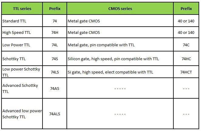
The prefixes for TTL and CMOS family ICs are listed below.
Some most used ICs for logic gate design are given below
Quad 2-input gates
- 74LS00 – Quad 2-input NAND Gate
- 74LS01 – Quad 2-Input NAND Gate, Open Collector Outputs
- 74LS02 – Quad 2-Input NOR Gate
- 74LS03 – Quad 2-input NAND Gate with open collector outputs
- 74LS08 – Quad 2-input AND Gate
- 74LS09 – Quad 2-input AND Gate with open collector outputs
- 74LS32 – Quad 2-input OR Gate
- 74LS132 – Quad 2-input NAND Gate with Schmitt trigger inputs
- 74LS37, 74LS32, 74LS28 – Quad 2-InpuT NOR Gates
- 74LS26 – Quad 2-InpuT NAND Gate, OC (15V)
- 74LS28 – Quad 2-InpuT NAND Gate with OC (15V)
- 74LS33 – Quad 2-InpuT NOR Gate, Open Collector Outputs
- 74LS38 – Quad 2-InpuT NOR Gate, Open Collector Outputs
- 74LS38 – Quad 2-Input NAND Gate, Open Collector Outputs
Triple 3-input gates
- 74 LS 10 – Triple 3-inpuT NAND
- 74 LS 11 – Triple 3-inpuT AND
- 74 LS 12 – Triple 3-inpuT NAND with open collector outputs
- 74 LS 27 – Triple 3-inpuT NOR
- 74LS15 – Triple 3-InpuT AND Gate, Open Collector Outputs
Dual 4-input gates
- 74LS13 – Dual 4-InpuT NAND Schmitt Triggers
- 74 LS 20 – dual 4-inpuT NAND
- 74 LS 21 – dual 4-inpuT AND, Open Collector Outputs
- 74LS22 – Dual 4-InpuT NAND Gate, Open Collector Outputs
- 74LS40 – Dual 4-InpuT NAND Gates
- 74LS30 – 8 input NAND gate
Hex NOT gates
- 74 LS 04 – hex NOT
- 74 LS 05 – hex NOT with open collector outputs
- 74 LS 14 – hex NOT with Schmitt Trigger inputs
- 74LS19 – NAND Schmitt Trigger, Totem Pole Output
- 74LS23 – 2x Four input NOR with Strobe
- 74LS25 – 2x Four input NOR with Strobe
- 74LS30 – 8-InpuT NAND Gate
- 74LS39 – 4x two input NAND, Open collector
