In this tutorial, we will learn about BJT configured as Common Base Amplifier. We will see different characteristics of a Common Base Amplifier like its Voltage Gain, Current Gain, Input and Output Resistance, etc.
Introduction
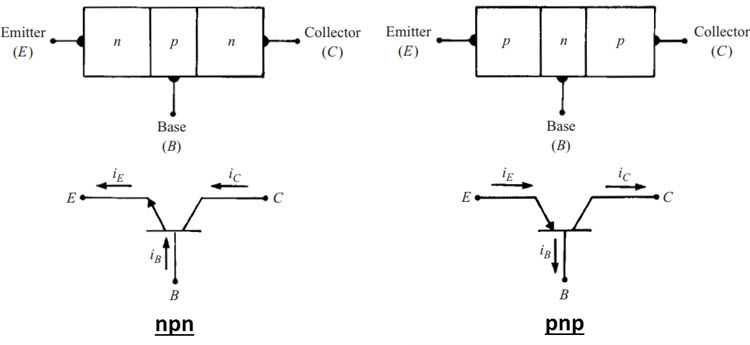
A Bipolar Junction Transistor or simply a BJT is a three terminal semiconductor device with alternating layers of n and p type semiconductor material. The three terminals, which correspond to the three regions of a transistor are called Emitter, Base and Collector.
The BJT can be of npn type of pnp type based on the configuration of the regions. Since both electrons and holes act as current carriers, the term “Bipolar” is used.
Basically, a BJT can be configured to work as an Amplifier or as a Switch. If a BJT is configured as an Amplifier, the amplitude of an electrical signal applied at the input is increased by several times at the output.
Configuring a BJT as a Switch is one of the common and frequently used applications of a Transistor. By operating the transistor in cut-off and saturation regions, you can implement an electronic switch using a Transistor.
Common Base Configuration
A Transistor can be configured in a two-port arrangement in three ways. They are Common Emitter Connection, Common Collector Connection and Common Base Connection. In common base configuration, the terminal is a common point to both input and output.
The following image shows both npn and pnp transistors in common base configuration. Irrespective of the type of transistor, the base terminal in common base configuration is always at ground potential.
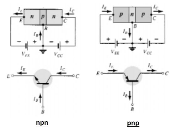
In common base configuration, the input variables are emitter current iE and base to emitter voltage VBE. Similarly, the output variables are the collector current iC and the base to collector voltage VCB.
To fully describe the characteristics of common base configuration like a Common Base Amplifier, you require two sets of characteristics.
- Input Characteristics (aka Driving point or Transfer characteristics)
- Output Characteristics (or collector characteristics)
The input characteristics will relate the input variables i.e. emitter current iE and base to emitter voltage VBE while the output variable VCB is held constant.
Coming to the output characteristics, they will relate the output variables i.e. collector current iC and base to collector voltage VCB while the input variable emitter current iE is held constant.
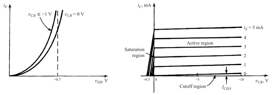
The output characteristics gives us the picture of three regions of operation of a transistor i.e. Cut-off, Active and Saturation.
Common Base Amplifier
An Amplifier is an Electronic Circuit, which increased the amplitude of an electrical signal. Electric power from the power supply is used to increase the amplitude of the signal. Gain of an amplifier is the quantity that determines the amount of amplification provided by the amplifier.
A simple amplifier circuit can be designed using a single transistor (either BJT or a FET) along with a few passive components. Single Transistor Amplifiers for BJT have three configurations. They are:
- Common Emitter Amplifier
- Common Collector Amplifier
- Common Base Amplifier
The focus of this tutorial is on Common Base Amplifier with its basic circuit and its performance characteristics i.e. voltage gain, current gain, input resistance and output resistance.
A typical Common Base Amplifier has the following topology.
- The input is given at the Emitter of the BJT.
- The output is taken from the Collector of the BJT.
- The base terminal, which is common to both input and output, is often connected to ground.
Common Base Amplifier Circuit
The following image shows a typical common base amplifier circuit with voltage divider bias configuration.
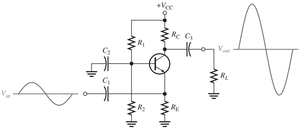
Base of the BJT is the common terminal and is at AC ground due to the capacitor. The input signal is given to the emitter through capacitor coupling. Output is taken at the collector and the load is capacitively coupled to the collector.
Characteristics of Common Base Amplifier
All the characteristics of a common base amplifier are explained with respect to r Parameters of the Transistor AC Model. Alternatively, you can use h parameters.
In order to determine the characteristics, we need to construct an AC equivalent model of the common base amplifier. The following image shows the same.
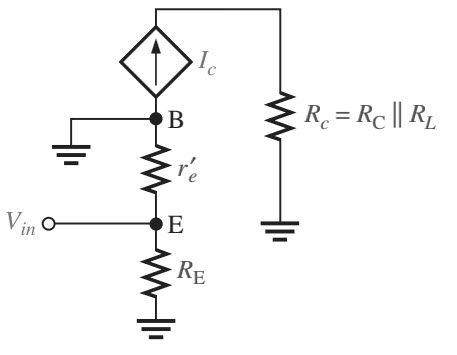
Voltage Gain
The voltage gain of CB amplifier from emitter (input) to collector (output) is given by
AV = Vout / Vin = Vc / Ve = Ic Rc / Ie (r’e || RE) ≈ Ie Rc / Ie (r’e || RE)
Assuming RE >> r’e, then AV ≈ Rc / r’e
Here, Rc = RC || RL
r’e = AC Emitter Resistance
the voltage gain of a common base amplifier is very high without the phase inversion.
Current Gain
The current gain of CB amplifier is output current divided by the input current. From AC equivalent mode, Ic is the output current and Ie is the input current.
Since Ic ≈ Ie, the current gain Ai ≈ 1.
Input Resistance
The input resistance is the equivalent resistance looking it at the emitter. It is given by
Rin = Vin / Iin = Ve / Ie = Ie (r’e || RE) / Ie = r’e || RE
Usually, RE is much greater than r’e.
If RE >> r’e, then Rin ≈ r’e.
This means that the input resistance of a common base amplifier is usually very low.
Output Resistance
The output resistance is the Thevenin equivalent at the output of the common base amplifier looking back into the amplifier. The AC collector resistance r’c is in parallel with RC and it is usually much larger than RC.
Hence, Rout ≈ RC
Conclusion
A Common Base Amplifier is less commonly used that common emitter amplifier. It is used to provide voltage gain without any current gain. It is used as a Voltage Amplifier or Buffer in some high frequency applications.
Based on the above analysis, we can conclude the following about a common base amplifier.
- It has relatively high voltage gain.
- Current gain is less than or sometimes approximately equal to 1.
- The input impedance is low.
- The output impedance is high.

One Response
A further article on how to compute the values of the resistors and capacitors would be really good.