In the 8051 Microcontroller Tutorial, we can see the Instruction Set and Addressing Modes. In this tutorial, we will take a look at the 8051 Microcontroller Special Function Registers or SFRs.
Internal RAM or Data Memory of the 8051 Microcontroller is divided into General Purpose Registers, Bit Addressable Registers, Register Banks and Special Function Registers. For detailed information, you can go through the 8051 Microcontroller Memory Organization Tutorial.
What Is Special Function Register In 8051?
8051 microcontroller has a dedicated set of Special Function Registers (SFRs) that control various functionalities and peripheral devices.
These registers are essential for programming the microcontroller’s behavior.
Special Function Registers in 8051 Microcontroller are used to program and control different hardware peripherals like Timers, Serial Port, I/O Ports etc. In fact, by manipulating the SFR in 8051 Microcontroller, you can assess or change the operating mode of the 8051 Microcontroller.
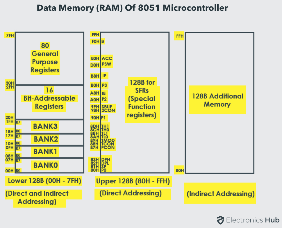
As a reminder, the following image shows you the basic structure of 8051 Microcontroller’s Internal RAM.
8051 Microcontroller Special Function Registers (SFRs)
Special Function Register in 8051 Microcontroller act as a control table that monitor and control the operation of the 8051 Microcontroller. If you observe in Internal RAM Structure, the Address Space from 80H to FFH is allocated to SFRs.
Out of these 128 Memory Locations (80H to FFH), there are only 21 locations that are actually assigned to SFRs. Each SFR has one Byte Address and also a unique name which specifies its purpose.
Since the SFRs are a part of the Internal RAM Structure, you can access SFRs as if you access the Internal RAM. The main difference is the address space: first 128 Bytes (00H to 7FH) is for regular Internal RAM and next 128 Bytes (80H to FFH) is for SFRs.
TIP: As only 21 of the possible 128 SFR memory locations are assigned, it is recommended that the remaining registers or memory locations are not accessed during programming.
Before going further, get an idea on 8051 MICROCONTROLLER ARCHITECTURE.
List of Special Function Registers In 8051 Microcontroller
- Accumulator (A)
- B Register (B)
- Program Status Word (PSW)
- Data Pointer (DPTR)
- Stack Pointer (SP)
- DPL (Data Pointer Low)
- DPH (Data Pointer High)
- Interrupt Enable Register (IE)
- Interrupt Priority Register (IP)
- I/O Port Registers (P0, P1, P2, P3)
- Power Control Register (PCON)
- Serial Control Register (SCON)
- SBUF (Serial Buffer Register)
- Timer/Counter Registers (TMOD, TH0, TL0, TH1, TL1)
Categories of 8051 Microcontroller Special Function Registers
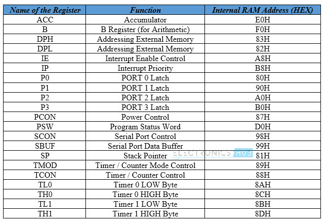
All the 21 8051 Microcontroller Special Function Registers (SFRs) along with their functions and Internal RAM Address is given in the following table.
There are many ways to categorize these 21 Special Function Registers but I find the following way as an appropriate one. The 21 Special Function Registers of 8051 Microcontroller are categorized in to seven groups.
Different Types of Special Function Registers (SFRs) in 8051 microcontroller:
- Math or CPU Registers: A and B
- Status Register: PSW (Program Status Word)
- Pointer Registers: DPTR (Data Pointer – DPL, DPH) and SP (Stack Pointer)
- I/O Port Latches: P0 (Port 0), P1 (Port 1), P2 (Port 2) and P3 (Port 3)
- Peripheral Control Registers: PCON, SCON, TCON, TMOD, IE and IP
- Peripheral Data Registers: TL0, TH0, TL1, TH1 and SBUF
8051 Microcontroller CPU or Math Registers:
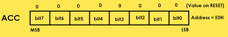
A or Accumulator (ACC)
The Accumulator or Register A is the most important and most used 8051 Microcontroller SFRs. The Register A is located at the address E0H in the SFR memory space. The Accumulator is used to hold the data for almost all the ALU Operations.
Some of the operations where the Accumulator is used are:
- Arithmetic Operations like Addition, Subtraction, Multiplication etc.
- Logical Operations like AND, OR, NOT etc.
- Data Transfer Operations (between 8051 and External Memory)
The name “Accumulator” came from the fact this register is used to accumulate (or store) the result of all Arithmetic and most of the Logical Operations.
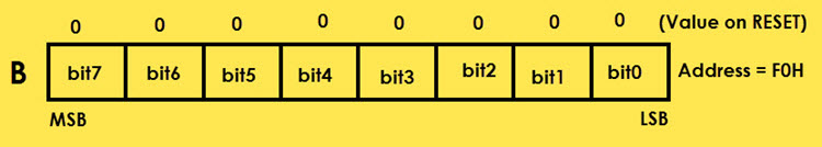
B (Register B)
The B Register is used along with the ACC in Multiplication and Division operations. These two operations are performed on data that are stored only in Registers A and B. During Multiplication Operation, one of the operand (multiplier or multiplicand) is stores in B Register and also the higher byte of the result.
In case of Division Operation, the B Register holds the divisor and also the remainder of the result. It can also be used as a General Purpose Register for normal operations and is often used as an Auxiliary Register by Programmers to store temporary results.
Register B is located at the address F0H of the SFR Address Space.
Program Status Word (PSW)
The PSW or Program Status Word Register is also called as Flag Register and is one of the important SFRs. The PSW Register consists of Flag Bits, which help the programmer in checking the condition of the result and also make decisions.
Flags are 1-bit storage elements that store and indicate the nature of the result that is generated by execution of certain instructions. The following image shows the contents of the PSW Register.
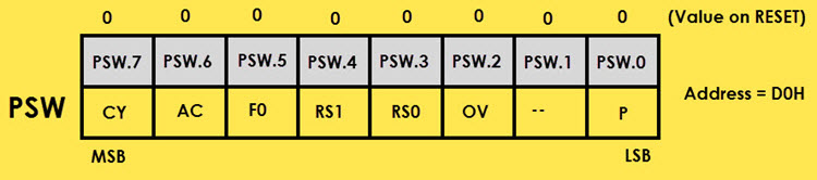
The following table describes the function of each flag.
Pointer Registers
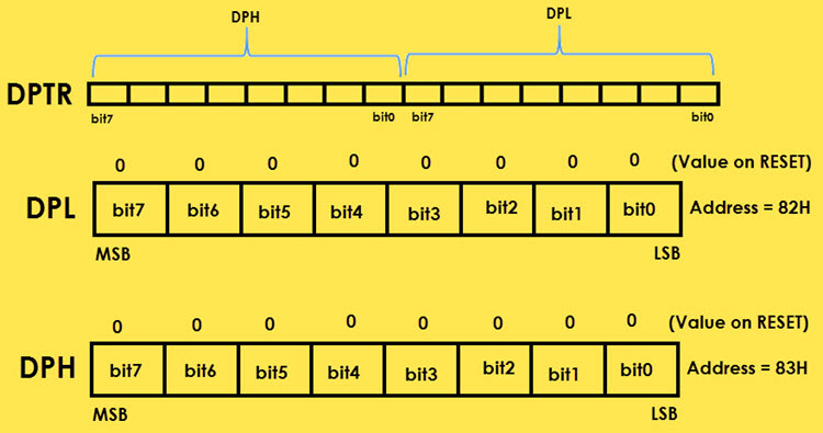
Data Pointer (DPTR – DPL and DPH)
The Data Pointer is a 16-bit Register and is physically the combination of DPL (Data Pointer Low) and DPH (Data Pointer High) SFRs. The Data Pointer can be used as a single 16-bit register (as DPTR) or two 8-bit registers (as DPL and DPH).
DPTR doesn’t have a physical Memory Address but the DPL (Lower Byte of DPTR) and DPH (Higher Byte of DPTR) have separate addresses in the SFR Memory Space. DPL = 82H and DPH = 83H.
The DPTR Register is used by the programmer addressing external memory (Program – ROM or Data – RAM).
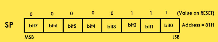
Stack Pointer (SP)
SP or Stack Pointer points out to the top of the Stack and it indicates the next data to be accessed. Stack Pointer can be accesses using PUSH, POP, CALL and RET Instructions. The Stack Pointer is an 8-bit register and upon reset, the Stack Pointer is initialized with 07H.
When writing a new data byte into the stack, the SP (Stack Pointer) is automatically incremented by 1 and the new data is written at an address SP+1. When reading data from stack, the data is retrieved from the Address in SP and after that the SP is decremented by 1 (SP-1).
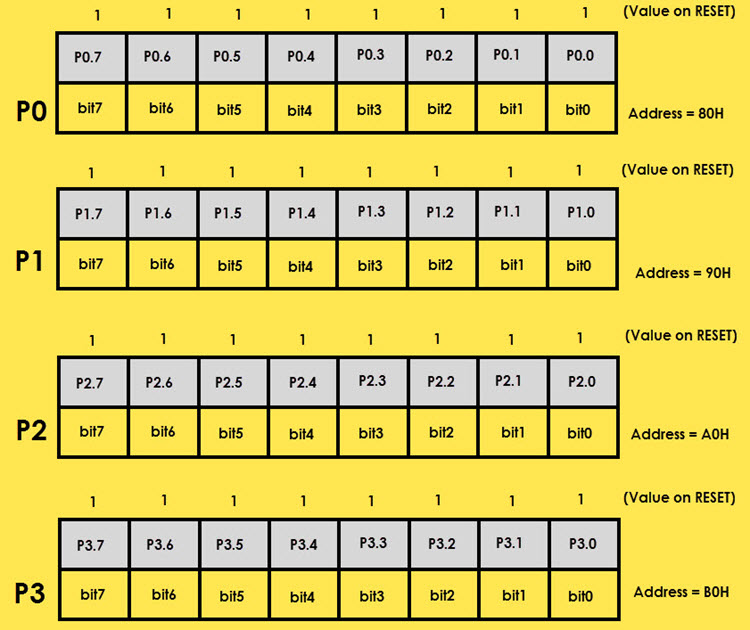
I/O Port Registers (P0, P1, P2 and P3)
The 8051 Microcontroller four Ports which can be used as Input and/or Output. These four ports are P0, P1, P2 and P3. Each Port has a corresponding register with same names (the Port Registers are also P0, P1, P2 and P3). The addresses of the Port Registers are as follows: P0 – 80H, P1 – 90H, P2 – A0H and P2 – B0H.
Each bit in these SFRs corresponds to one physical Pin in the 8051 Microcontroller. All these Port Registers are both Bit Addressable and Byte Addressable. Writing 1 or 0 on a Port Register Bit will reflect as an appropriate voltage (5V and 0V) on the corresponding Pin.
If a Port Bit is SET (declared as 1), the corresponding Port Pin will be configured as Input and similarly if a Port Bit is CLEARED (declared as 0), the corresponding Port Pin is configured as Output. Upon reset, all the Port Bits are SET (1) and hence, all the Port Pins are configured as Inputs.
Draw And Explain Port Structure With SFRs Used In Programming
Peripheral Control Registers
PCON (Power Control)
The PCON or Power Control register, as the name suggests is used to control the 8051 Microcontroller’s Power Modes and is located at 87H of the SFR Memory Space. Using two bits in the PCON Register, the microcontroller can be set to Idle Mode and Power Down Mode.
NOTE: PCON register is not bit addressable.
During Idle Mode, the Microcontroller will stop the Clock Signal to the ALU (CPU) but it is given to other peripherals like Timer, Serial, Interrupts, etc. In order to terminate the Idle Mode, you have to use an Interrupt or Hardware Reset.
In the Power Down Mode, the oscillator will be stopped and the power will be reduced to 2V. To terminate the Power Down Mode, you have to use the Hardware Reset.
Apart from these two, the PCON Register can also be used for few additional purposes. The SMOD Bit in the PCON Register is used to control the Baud Rate of the Serial Port.
There are two general purpose Flag Bits in the PCON Register, which can be used by the programmer during execution.

The following table describes the function of each bit in the PCON Register.
|
Bit |
Symbol | Description | Additional Info |
| 7 | SMOD | Serial Comm. Baud Rate Modify Bit |
If 1, doubles the baud rate using Timer 1. If 0, normal timer 1 baud rate. |
|
6 – 4 |
—- | — | |
|
3 |
GF1 |
General Purpose User Flag (Bit 1) |
|
| 2 | GF0 | General Purpose User Flag (Bit 0) |
|
|
1 |
PD | Power Down Bit | To enter Power Down Mode, set to 1 |
| 0 | IDL | Idle Mode Bit |
To enter Idle Down Mode, set to 1 |
SCON (Serial Control)
The Serial Control or SCON SFR is used to control the 8051 Microcontroller’s Serial Port. It is located as an address of 98H. Using SCON, you can control the Operation Modes of the Serial Port, Baud Rate of the Serial Port and Send or Receive Data using Serial Port.
SCON Register also consists of bits that are automatically SET when a byte of data is transmitted or received.
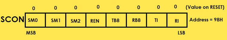
The following table describes the function of each bit in the SCON Register.
|
Bit |
Symbol | Description |
| 7 | SM0 |
Serial Port Mode Selection Bit 0 |
|
6 |
SM1 | Serial Port Mode Selection Bit 1 |
| 5 | SM2 |
Multiprocessor Comm. Bit |
|
4 |
REN | Receive Enable Bit |
| 3 | TB8 |
Transmitted Bit 8 |
|
2 |
RB8 | Received Bit 8 |
| 1 | TI |
Transmit Interrupt Flag |
|
0 |
RI |
Receive Interrupt Flag |
The Serial Port Mode Selection Bits (SM0 and SM1) determine the mode of UART and also the baud rate. The following table gives an overview of how the Serial Port Mode Selection Bits can be used to configure Serial Port (UART) of 8051.
Serial Port Mode Selection Bits
|
SM0 |
SM1 | Mode | Description | Baud Rate |
| 0 | 0 | 0 | 8-Bit Synchronous Shift Register Mode |
Fixed Baud Rate (Frequency of oscillator / 12) |
|
0 |
1 | 1 | 8-bit Standard UART
mode |
Variable Baud Rate (Can be set by Timer 1) |
| 1 | 0 | 2 | 9-bit Multiprocessor Comm. mode |
Fixed Baud Rate (Frequency of oscillator / 32 or Frequency of oscillator / 64 |
|
1 |
1 | 3 | 9-bit Multiprocessor Comm. mode |
Variable Baud Rate (Can be set by Timer 1) |
TCON (Timer Control)
Timer Control or TCON Register in 8051 Microcontroller is used to start or stop the Timers. It also contains bits to indicate if the Timers has overflowed. The TCON SFR also consists of Interrupt related bits.
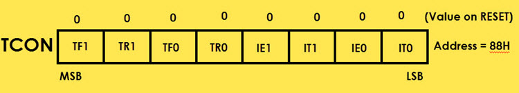
The following table gives the explanation of each bit in the TCON Register in 8051.
|
Bit |
Symbol | Description |
Additional Info |
|
7 |
TF1 | Timer 1 Overflow Flag | Set when Timer 1 overflows (all 1s to 0). Cleared when processor executes ISR at 001BH. |
| 6 | TR1 | Timer 1 Run Control Bit |
To enable Timer/Counter, set to 1. Clear to halt the timer. |
|
5 |
TF0 | Timer 0 Overflow Flag | Set when Timer 0 overflows (all 1s to 0). Cleared when processor executes ISR at 000BH. |
| 4 | TR0 | Timer 0 Run Control Bit |
To enable Timer/Counter, set to 1. Clear to halt the timer. |
|
3 |
IE1 | Ext. Interrupt 1 Edge Flag | Set when HIGH to LOW is received on INT1 (P3.3). Cleared when processor executes ISR at 0013H. |
| 2 | IT1 | Ext. Interrupt 1 Type Control Bit |
If 1, Interrupt 1 occurs on falling edge. If 0, Interrupt 1 occurs on low level. |
|
1 |
IE0 | Ext. Interrupt 0 Edge Flag | Set to 1 when HIGH to LOW is received on INT0 (P3.2). Cleared when processor executes ISR at 0003H. |
| 0 | IT0 | Ext. Interrupt 0 Type Control Bit |
If 1, Interrupt 0 occurs on falling edge. If 0, Interrupt 0 occurs on low level. |
TMOD (Timer Mode)
The TMOD or Timer Mode register or SFR is used to set the Operating Modes of the Timers T0 and T1. The lower four bits are used to configure Timer0 and the higher four bits are used to configure Timer1.
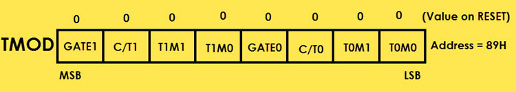
The following table explain about each bit in the TMOD SFR in 8051.
|
Bit |
Symbol |
Description |
|
7 / 3 |
Gate | OR Gate Enable Bit |
| 6 / 2 | C/Tx |
Select Timer or Counter Mode |
|
5 / 1 |
TxM1 | Timer / Counter Operating Mode Select Bit 1 |
| 4 / 0 | TxM0 |
Timer / Counter Operating Mode Select Bit 0 |
The Gatex bit is used to operate the Timerx with respect to the INTx pin or regardless of the INTx pin.
- GATE1 = 1 ==> Timer1 is operated only if TR1 (in TCON) is SET and Signal on INT1 is HIGH.
- GATE1 = 0 ==> Timer1 is operated irrespective of Signal on INT1 pin but TR1 (in TCON) must be SET.
- GATE0 = 1 ==> Timer0 is operated only if TR0 (in TCON) is SET and Signal on INT0 is HIGH.
- GATE0 = 0 ==> Timer0 is operated irrespective of Signal on INT0 pin but TR0 (in TCON) must be SET.
The C/Tx bit is used selects the source of pulses for the Timer to count.
- C/T1 = 1 ==> Timer1 counts pulses from Pin T1 (P3.5) (Counter Mode)
- C/T1 = 0 ==> Timer1 counts pulses from internal oscillator (Timer Mode)
- C/T0 = 1 ==> Timer0 counts pulses from Pin T0 (P3.4) (Counter Mode)
- C/T0 = 0 ==> Timer0 counts pulses from internal oscillator (Timer Mode)
|
TxM0 |
TxM1 | Mode |
Description |
|
0 |
0 | 0 | 13-bit Timer Mode (THx – 8-bit and TLx – 5-bit) |
|
0 |
1 | 1 | 16-bit Timer Mode |
| 1 | 0 | 2 |
8-bit Auto Reload Timer Mode |
| 1 | 1 | 3 |
Two 8-bit Timer Mode or Split Timer Mode |
NOTE: x = 0 for Timer 0 and x = 1 for Timer 1.
IE (Interrupt Enable)
The IE or Interrupt Enable Register is used to enable or disable individual interrupts. If a bit is SET, the corresponding interrupt is enabled and if the bit is cleared, the interrupt is disabled. The Bit7 of the IE register i.e., EA bit is used to enable or disable all the interrupts.
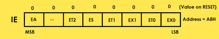
The following table describes the functions of each bit in the IE Register.
|
Bit |
Symbol | Description |
Additional Info |
|
7 |
EA | Global Interrupt Enable Bit. | If set to 1, individual interrupts can be enabled. If set to 0, all interrupts are disabled. |
| 6 | — |
— |
|
|
5 |
ET2 | Reserved | |
| 4 | ES | Serial Port Interrupt Enable Bit |
If set to 1, Serial Port interrupt is enabled. If set to 0, Serial Port interrupt is disabled. |
|
3 |
ET1 | Timer 1 Overflow Interrupt Enable Bit | If set to 1, Timer 1 Overflow interrupt is enabled. If set to 0, Timer 1 Overflow interrupt is disabled. |
| 2 | EX1 | Ext. Interrupt 1 Enable Bit |
If set to 1, Ext. Interrupt 1 is enabled. If set to 0, Ext. Interrupt 1 is disabled. |
|
1 |
ET0 | Timer 0 Overflow Interrupt Enable Bit | If set to 1, Timer 0 Overflow interrupt is enabled. If set to 0, Timer 0 Overflow interrupt is disabled. |
| 0 | EX0 | Ext. Interrupt 0 Enable Bit |
If set to 1, Ext. Interrupt 0 is enabled. If set to 0, Ext. Interrupt 0 is disabled. |
NOTE: The Interrupt Enable (IE) SFR is bit addressable.
IP (Interrupt Priority)
The IP or Interrupt Priority Register is used to set the priority of the interrupt as High or Low. If a bit is CLEARED, the corresponding interrupt is assigned low priority and if the bit is SET, the interrupt is assigned high priority.
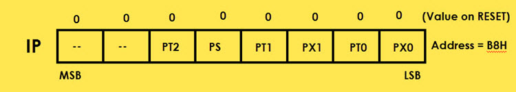
The following table describes the functions of each bit in the IP Register.
|
Bit |
Symbol |
Description |
|
7 |
— | — |
| 6 | — |
— |
|
5 |
PT2 | Reserved |
| 4 | PS |
Priority of Serial Port Interrupt |
|
3 |
PT1 | Priority of Timer 1 Overflow Interrupt |
| 2 | PX1 |
Priority of Ext. Interrupt 1 |
|
1 |
PT0 | Priority of Timer 0 Overflow Interrupt |
| 0 | PX0 |
Priority of Ext. Interrupt 0 |
NOTE: The Interrupt Priority (IP) SFR is bit addressable.
Peripheral Data Registers
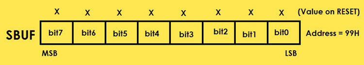
SBUF (Serial Data Buffer)
The Serial Buffer or SBUF register in 8051 is used to hold the serial data while transmission or reception. This 8-bit register acts as a temporary storage location for data being transmitted or received through the microcontroller’s serial port. Data written to SBUF is sent out serially, and data received serially is stored in SBUF before being processed further.
TL0/TH0 (Timer 0 Low/High)
The Timer 0 consists of two SFRs: TL0 and TH0. The TL0 is the lower byte and the TH0 is the higher byte and together they form a 16-bit Timer0 Register.
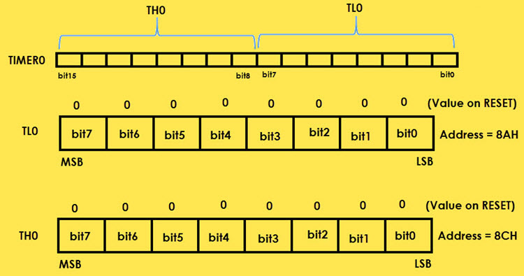
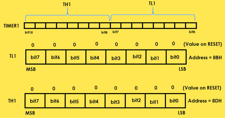
TL1/TH1 (Timer 1 Low/High)
The TL1 and TH1 are the lower and higher bytes of the Timer 0.
In this tutorial, we have seen the 8051 Microcontroller Special Function Registers (SFRs), their addresses, structures, reset values etc.
FAQs: SFRs in 8051 Microcontroller
How many SFRs are present in an 8051 microcontroller?
There are 21 Special Function Registers (SFRs) in an 8051 microcontroller. SFRs are located in the upper memory space (address range 0x80 to 0xFF) of the 8051’s internal memory.
In which memory space are SFRs located in an 8051 microcontroller?
Special Function Registers (SFRs) are located in the upper memory space of the 8051 microcontroller, specifically from address 0x80 to 0xFF.
Which registers in the 8051 microcontroller can be accessed at the bit level?
The Accumulator (A), the B register, the Port registers (P0, P1, P2, P3), and the Interrupt Enable (IE) register are bit-addressable in the 8051 microcontroller. This means you can access and manipulate individual bits within these registers.
Which registers in the 8051 microcontroller can be accessed as a complete byte?
Most registers in the 8051 microcontroller, including the Special Function Registers (SFRs), are byte-addressable. This means you can access and manipulate all eight bits of the register at once. Some examples include the Timer registers (T0, T1), Serial Communication registers (SCON, SBUF), and the Stack Pointer (SP).
What Is the role of the IE register in interrupt handling within an 8051 microcontroller?
The IE (Interrupt Enable) register in the 8051 microcontroller controls which interrupts are allowed to interrupt the main program. Each bit in the IE register corresponds to a specific interrupt source. By setting a bit to 1, you enable the corresponding interrupt, allowing it to trigger an interrupt service routine (ISR) when the interrupt condition is met. Conversely, setting a bit to 0 disables the interrupt.

7 Responses
Thank you for simple explain i easy to understand
Explanation in usage of each bits can be helpful to understand deeper, please add those
Many thanks to u for making it understandable.
Nicely presented content…. Best for the Revision of basic concept.
Nice sir really a good concept
good to skim before exam
Really nice