In the previous tutorial on 8051 Microcontroller, we have seen the 8051 Microcontroller Introduction and Basics, Pin Diagram, Pin Description and the Architecture overview. In this tutorial, we will continue exploring 8051 Microcontroller by understanding the 8051 Microcontroller Memory Organization, Program Memory (ROM), Data Memory (RAM), External Memory.
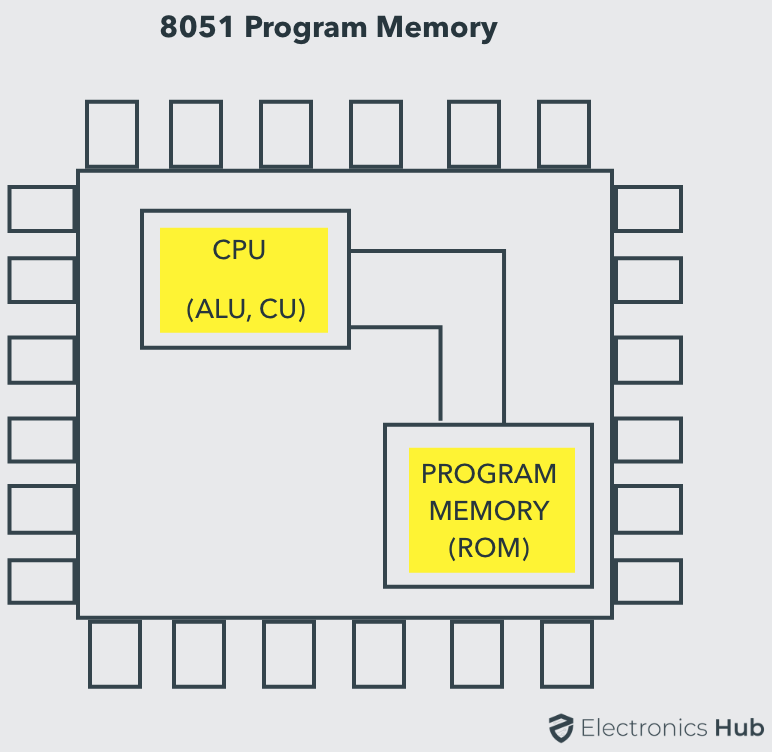
When the differences between microprocessor and microcontroller are mentioned in the previous tutorial, the main difference can be stated as on-chip memory i.e., a Microcontroller has both Program Memory (ROM) and Data Memory (RAM) on the same chip (IC), whereas a Microprocessor has to be externally interface with the memory modules.
Hence, it is clear that the memory is an important part of the 8051 Microcontroller Architecture (for that matter, any Microcontroller). So, it is important for us to understand the 8051 Microcontroller Memory Organization i.e., how memory is organized, how the processor accesses each memory and how to interface external memory with 8051 Microcontroller.
Before going in to the details of the 8051 Microcontroller Memory Organization, we will first see a little bit about the Computer Architecture and then proceed with memory organization of 8051 Microcontroller.
Also read about 8051 MICROCONTROLLER ARCHITECTURE OVERVIEW.
Outline
ToggleTypes of Computer Architecture
Basically, Microprocessors or Microcontrollers are classified based on the two types of Computer Architecture: Von Neumann Architecture and Harvard Architecture.
Von Neumann Architecture
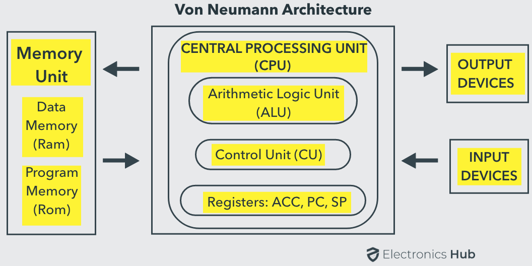
Von Neumann Architecture or Princeton Architecture is a Computer Architecture, where the Program i.e., the Instructions and the Data are stored in a single memory.
Since the Instruction Memory and the Data Memory are the same, the Processor or CPU cannot access both Instructions and Data at the same time as they use a single bus.
This type of architecture has severe limitations to the performance of the system as it creates a bottleneck while accessing the memory.
Harvard Architecture
Harvard Architecture, in contrast to Von Neumann Architecture, uses separate memory for Instruction (Program) and Data. Since the Instruction Memory and Data Memory are separate in a Harvard Architecture, their signal paths i.e., buses are also different and hence, the CPU can access both Instructions and Data at the same time.
Almost all Microcontrollers, including 8051 Microcontroller implement Harvard Architecture.
8051 Microcontroller Memory Organization
The 8051 Microcontroller Memory is separated in Program Memory (ROM) and Data Memory (RAM). The Program Memory of the 8051 Microcontroller is used for storing the program to be executed i.e., instructions. The Data Memory on the other hand, is used for storing temporary variable data and intermediate results.
8051 Microcontroller has both Internal ROM and Internal RAM. If the internal memory is inadequate, you can add external memory using suitable circuits.
Read this interesting post: 8051 MICROCONTROLLER PROJECTS FOR ENGINEERING STUDENTS.
Program Memory (ROM) of 8051 Microcontroller
In 8051 Microcontroller, the code or instructions to be executed are stored in the Program Memory, which is also called as the ROM of the Microcontroller. The original 8051 Microcontroller by Intel has 4KB of internal ROM.
Some variants of 8051 like the 8031 and 8032 series doesn’t have any internal ROM (Program Memory) and must be interfaced with external Program Memory with instructions loaded in it.
Almost all modern 8051 Microcontrollers, like 8052 Series, have 8KB of Internal Program Memory (ROM) in the form of Flash Memory (ROM) and provide the option of reprogramming the memory.
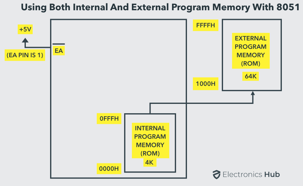
In case of 4KB of Internal ROM, the address space is 0000H to 0FFFH. If the address space i.e., the program addresses exceed this value, then the CPU will automatically fetch the code from the external Program Memory.
For this, the External Access Pin (EA Pin) must be pulled HIGH i.e., when the EA Pin is high, the CPU first fetches instructions from the Internal Program Memory in the address range of 0000H to 0FFFFH and if the memory addresses exceed the limit, then the instructions are fetched from the external ROM in the address range of 1000H to FFFFH.
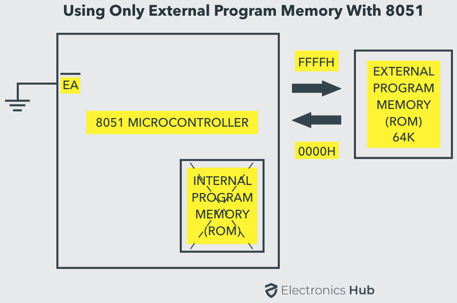
There is another way to fetch the instructions: ignore the Internal ROM and fetch all the instructions only from the External Program Memory (External ROM). For this scenario, the EA Pin must be connected to GND. In this case, the memory addresses of the external ROM will be from 0000H to FFFFH.
Data Memory (RAM) of 8051 Microcontroller
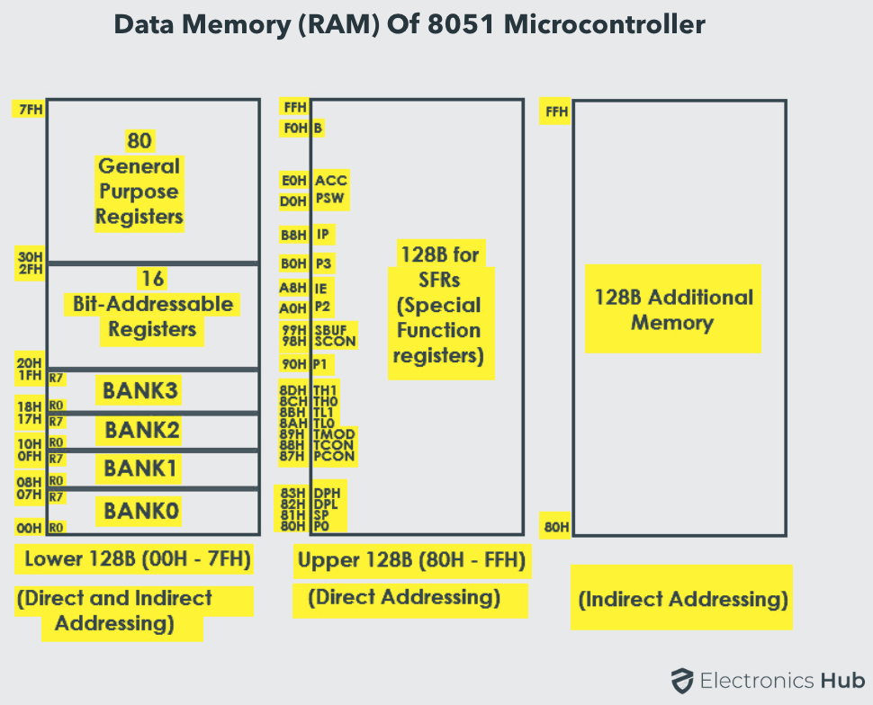
The Data Memory or RAM of the 8051 Microcontroller stores temporary data and intermediate results that are generated and used during the normal operation of the microcontroller. Original Intel’s 8051 Microcontroller had 128B of internal RAM.
But almost all modern variants of 8051 Microcontroller have 256B of RAM. In this 256B, the first 128B i.e., memory addresses from 00H to 7FH is divided in to Working Registers (organized as Register Banks), Bit – Addressable Area and General Purpose RAM (also known as Scratchpad area).
In the first 128B of RAM (from 00H to 7FH), the first 32B i.e., memory from addresses 00H to 1FH consists of 32 Working Registers that are organized as four banks with 8 Registers in each Bank.
The 4 banks are named as Bank0, Bank1, Bank2 and Bank3. Each Bank consists of 8 registers named as R0 – R7. Each Register can be addressed in two ways: either by name or by address.
To address the register by name, first the corresponding Bank must be selected. In order to select the bank, we have to use the RS0 and RS1 bits of the Program Status Word (PSW) Register (RS0 and RS1 are 3rd and 4th bits in the PSW Register).
When addressing the Register using its address i.e., 12H for example, the corresponding Bank may or may not be selected. (12H corresponds to R2 in Bank2).
The next 16B of the RAM i.e., from 20H to 2FH are Bit – Addressable memory locations. There are totally 128 bits that can be addressed individually using 00H to 7FH or the entire byte can be addressed as 20H to 2FH.
For example 32H is the bit 2 of the internal RAM location 26H.
The final 80B of the internal RAM i.e., addresses from 30H to 7FH, is the general purpose RAM area which are byte addressable.
These lower 128B of RAM can be addressed directly or indirectly.
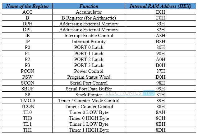
The upper 128B of the RAM i.e., memory addresses from 80H to FFH is allocated for Special Function Registers (SFRs). SFRs control specific functions of the 8051 Microcontroller. Some of the SFRs are I/O Port Registers (P0, P1, P2 and P3), PSW (Program Status Word), A (Accumulator), IE (Interrupt Enable), PCON (Power Control), etc.
SRFs Memory addresses are only direct addressable. Even though some of the addresses between 80H and FFH are not assigned to any SFR, they cannot be used as additional RAM area.
In some microcontrollers, there is an additional 128B of RAM, which share the memory address with SFRs i.e., 80H to FFH. But, this additional RAM block is only accessed by indirect addressing.
Interfacing External Memory with 8051 Microcontroller
It is always good to have an option to expand the capabilities of a Microcontroller, whether it is in terms of Memory or IO or anything else. Such expansion will be useful to avoid design throttling. We have seen that a typical 8051 Microcontroller has 4KB of ROM and 128B of RAM (most modern 8051 Microcontroller variants have 8K ROM and 256B of RAM).
The designer of an 8051 Microcontroller based system is not limited to the internal RAM and ROM present in the 8051 Microcontroller. There is a provision of connecting both external RAM and ROM i.e., Data Memory and Program.
The reason for interfacing external Program Memory or ROM is that complex programs written in high – level languages often tend to be larger and occupy more memory.
Another important reason is that chips like 8031 or 8032, which doesn’t have any internal ROM, have to be interfaced with external ROM.
A maximum of 64KB of Program Memory (ROM) and Data Memory (RAM) each can be interface with the 8051 Microcontroller.
The following image shows the block diagram of interfacing 64KB of External RAM and 64KB of External ROM with the 8051 Microcontroller.
An important point to remember when interfacing external memory with 8051 Microcontroller is that Port 0 (P0) cannot be used as an IO Port as it will be used for multiplexed address and data bus (A0 – A7 and D0 – D7). Not always, but Port 2 may be used as higher byte of the address bus.
In this tutorial, we have seen the 8051 Microcontroller Memory Organization, Program Memory, Data Memory, Internal ROM and RAM and how to interface external Memory (ROM and RAM) with 8051 Microcontroller.




10 Responses
A very well done explanation, I was really struggling with understanding the internal memory of 8051, this made everything clear, Thanks.
which instruction is used to fetch the code from external ROM
use DPTR for accessing external memory.
can I get the explanation about various interrupts and its programming in 8051
Very nice and helpful
Movc and address location to be fetch
Very much helpfull… Thank you sir..
which instruction is used to fetch the code from external RAM
hello,very nice presentation , ihave a qust , in the adress RAM i.e 000FH , the H refere to Hexadecimal ?
and is all RAM adresses are in 4 bit format ?
Thanks So much for this Article I am Currently a Diploma Pursing Student,it helps me alot.