In the previous 8051 tutorial, we have seen the basics of 8051 Microcontroller like its history, features, packaging and few applications. In this tutorial, we will continue further by looking at the 8051 Microcontroller Pin Diagram and 8051 Microcontroller Pin Description along with some other details like the basic circuit of the 8051 Microcontroller.
8051 Microcontroller Pin Diagram and Pin Description
We will first see the 8051 Microcontroller Pin Diagram and Pin Description as it will be easier to understand the architecture later (in the next tutorial). Pin Diagram or Pin out of a device will specify the pins of an electrical connector along with its functions.
Before going to the 8051 Microcontroller Pin Diagram, read the Introduction to 8051 Microcontroller.
8051 Microcontroller Pin Diagram
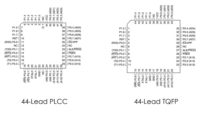
As mentioned in the previous tutorial, 8051 Microcontroller is available in a variety of packages like 40 – pin DIP or 44 – lead PLCC and TQFP. The pin orientation of an 8051 Microcontroller may change with the package but the Pin Configuration is same.
The following image shows the 8051 Microcontroller Pin Diagram with respect to a 40 – pin Dual In-line Package (DIP).
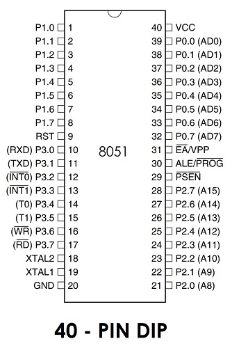
Since it is a 40 – pin DIP IC, each side contains 20 Pins. We have also seen that there other packages of 8051 like the 44 – Lead PLCC and the 44 – Lead TQFP. The following image shows the 8051 Microcontroller Pin Diagram for these packages specifically.
Now that we have seen the 8051 Microcontroller Pin Diagram, we need to understand the functions of these pins. Hence, we will now see the 8051 Microcontroller Pin Description.
8051 Microcontroller Pin Description
The Pin Description or Pin Configuration of the 8051 Microcontroller will describe the functions of each pins of the 8051 Microcontroller. Let us now see the pin description.
Pins 1 – 8 (PORT 1): Pins 1 to 8 are the PORT 1 Pins of 8051. PORT 1 Pins consists of 8 – bit bidirectional Input / Output Port with internal pull – up resistors. In older 8051 Microcontrollers, PORT 1 doesn’t serve any additional purpose but just 8 – bit I/O PORT.
In some of the newer 8051 Microcontrollers, few PORT 1 Pins have dual functions. P1.0 and P1.1 act as Timer 2 and Timer 2 Trigger Input respectively.
P1.5, P1.6 and P1.7 act as In-System Programming Pins i.e. MOSI, MISO and SCK respectively.
Pin 9 (RST): Pin 9 is the Reset Input Pin. It is an active HIGH Pin i.e. if the RST Pin is HIGH for a minimum of two machine cycles, the microcontroller will be reset. During this time, the oscillator must be running.
Pins 10 – 17 (PORT 3): Pins 10 to 17 form the PORT 3 pins of the 8051 Microcontroller. PORT 3 also acts as a bidirectional Input / Output PORT with internal pull-ups. Additionally, all the PORT 3 Pins have special functions. The following table gives the details of the additional functions of PORT 3 Pins.
PORT 3 Pin
Function
Description
P3.0
RXD
Serial Input
P3.1
TXD
Serial Output
P3.2
External Interrupt 0
P3.3
External Interrupt 1
P3.4
T0
Timer 0
P3.5
T1
Timer 1
P3.6
External Memory Write
P3.7
External Memory Read
Pins 18 & 19: Pins 18 and 19 i.e. XTAL 2 and XTAL 1 are the pins for connecting external oscillator. Generally, a Quartz Crystal Oscillator is connected here.
Pin 20 (GND): Pin 20 is the Ground Pin of the 8051 Microcontroller. It represents 0V and is connected to the negative terminal (0V) of the Power Supply.
Pins 21 – 28 (PORT 2): These are the PORT 2 Pins of the 8051 Microcontroller. PORT 2 is also a Bidirectional Port i.e. all the PORT 2 pins act as Input or Output. Additionally, when external memory is interfaced, PORT 2 pins act as the higher order address byte. PORT 2 Pins have internal pull-ups.
Pin 29 (PSEN): Pin 29 is the Program Store Enable Pin (PSEN). Using this pins, external Program Memory can be read.
Pin 30 (ALE/PROG): Pin 30 is the Address Latch Enable Pin. Using this Pins, external address can be separated from data (as they are multiplexed by 8051).
During Flash Programming, this pin acts as program pulse input (PROG).
Pin 31 (EA/VPP): Pin 31 is the External Access Enable Pin i.e. allows external Program Memory. Code from external program memory can be fetched only if this pin is LOW. For normal operations, this pins is pulled HIGH.
During Flash Programming, this Pin receives 12V Programming Enable Voltage (VPP).
Pins 32 – 39 (PORT 0): Pins 32 to 39 are PORT 0 Pins. They are also bidirectional Input / Output Pins but without any internal pull-ups. Hence, we need external pull-ups in order to use PORT 0 pins as I/O PORT.
In addition to acting as I/O PORT, PORT 0 also acts as lower order address/data bus when external memory is accessed.
Pin 40 (VCC): Pin 40 is the power supply pin to which the supply voltage is given (+5V).
8051 Microcontroller Basic Circuit
Now that we have seen the 8051 Microcontroller Pin Diagram and corresponding Pin Description, we will proceed to the basic circuit or schematic of the 8051 Microcontroller. The following image shows the basic circuit of the 8051 Microcontroller.
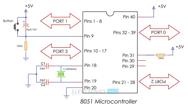
This basic circuit of 8051 microcontroller is the minimal interface required for it to work. The basic circuit includes a Reset Circuit, the oscillator circuit and power supply. Let us discuss a little bit deeper about this basic circuit of 8051 Microcontroller.
First is the power supply. Pins 40 and 20 (VCC and GND) of the 8051 Microcontroller are connected to +5V and GND respectively.
Next is the Reset Circuit. A logic HIGH (+5V) on Reset Pin for a minimum of two machine cycles (24 clock cycles) will reset the 8051 Microcontroller. The reset circuit of the 8051 Microcontroller consists of a capacitor, a resistor and a push button and this type of reset circuit provides a Manual Reset Option. If you remove the push button, then the reset circuit becomes a Power-On Reset Circuit.
The next part of the basic circuit of the 8051 Microcontroller is the Oscillator Circuit or the Clock Circuit. A Quartz Crystal Oscillator is connected across XTAL1 and XTAL2 pins i.e. Pins 19 and 18. The capacitors C1 and C2 can be selected in the range of 20pF to 40pF.
As mentioned in the 8051 Microcontroller Pin Description, PORTS 1, 2 and 3, all have internal pull – ups and hence can be directly used as Bidirectional I/O Ports. But, we need to add external Pull – ups for PORT 0 Pins in order to use it as an I/O Port.
Generally, a 1KΩ Resistor Pack of 8 Resistors is used as a Pull – up for the PORT 0 of the 8051 Microcontroller.
In this tutorial, we have seen about the 8051 Microcontroller Pin Diagram, Pin Description and the Basic Circuit of 8051 Microcontroller. In the next tutorial, we will continue with the architecture and few other features of 8051 Microcontroller.

6 Responses
Real good explanation. Complete and precise.
Excellent Tutorial. Thank you.
fabulous
good and understandable
Its very nice and easy to understand
Good explanation with diagrams and neatly presented…. ????