In this tutorial, we will learn about an introduction to semiconductors as they are an essential part of Electronics. Before understanding several devices like Semiconductor Diodes, Transistors, etc. it is important to know a little bit about the electrical conductivity, energy gap and basic types of semiconductors.
This part of the tutorial will lay out a key foundation in easily learning the PN Junction, which is next in line.
Introduction
There are two types of semiconductor components in electronic and electrical circuits. They are active and passive components. Diodes are the foremost active components and resistors are the foremost passive components in electronic design circuits. Diodes are essentially unidirectional devices having exponential relationship for the current-voltage characteristics are made from semiconductor materials.
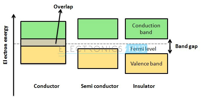
The three necessary materials that are utilized in electronics are insulators, semiconductors and conductors. These materials are classified in terms of electrical phenomenon. Electrical resistivity conjointly known as electrical resistance is a measure of how efficiently a material refuses the electrical current to flow through it.
The quality unit of the electrical resistivity is the ohm meter [Ω m]. A material with low electrical resistivity indicates the effective movement of electrical charge throughout the semiconductor.
Semiconductors are the materials whose resistivity values are in between insulators and conductors. These materials are neither smart insulators nor smart conductors. They have only a few free electrons because their atoms are tightly bonded in an exceedingly crystalline form are referred to as a “crystal lattice”. Samples of semiconductors are silicon and germanium.
Semiconductors have high importance in the manufacture of electronic circuits and integrated devices. The conductivity of semiconductors can be altered easily by varying the temperature and concentration of doping in the fabrication process. The capability to conduct electricity in semiconductor materials is considerably increased by a adding definite quantity of impurities to the crystalline lattice producing additional free electrons than holes.
The properties of semiconductor materials change considerably by adding small amounts of impurities to it. The process of shifting the balance between electrons and holes by incorporating impurity atoms in the silicon crystal lattice is called as doping. These impurity atoms are known as dopants. Based on the type of doping material incorporated, semiconductor crystals are classified into two types particularly n-type semiconductors and p-type semiconductors.
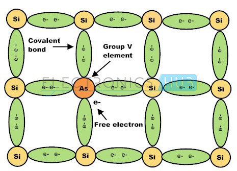
Group –V elements such as phosphorus, antimony and arsenic are usually classified as N-type impurities. These elements have five valence electrons. When N-type impurities are doped into silicon crystal, four of the five valence electrons form four strong covalent bonds with adjacent crystal atoms leaving one free electron.
Likewise, every N-type impurity atom produces a free electron in the conduction band which will drift to conduct electric current if a potential is applied to the material. N-type semiconductors can also be referred as Donors.
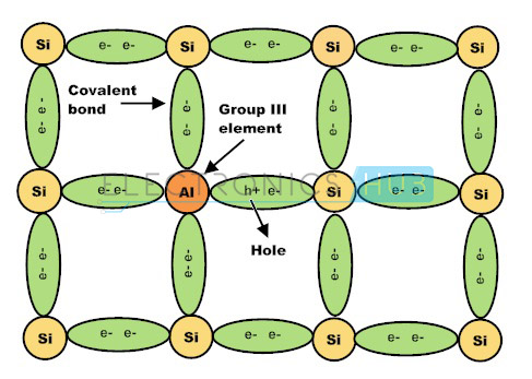
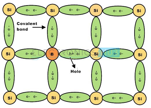
Group–III elements such as boron, aluminium, gallium and indium are usually classified as P-type impurities. These elements have three valence electrons. When P-type impurities are doped into silicon crystal, all the three valence electrons form three strong covalent bonds with adjacent crystal atoms.
There is a deficit of electrons to form the fourth covalent bond and this deficiency is termed as holes. Likewise, every P-type impurity atom produces a hole in the valence band which will drift to conduct electric current if a potential is applied to the material. P-type semiconductors can also be referred as Acceptors.
Resistivity
A characteristic property of every material that is helpful in comparing different materials on the basis of their ability to conduct electric current is known as electrical resistivity. Resistivity can be approximated by multiplying the resistance R of an electrical wire and the cross sectional area A, divided by the length of the wire L.
Conductivity, that is reciprocal of the electrical resistivity conjointly characterizes the materials how well they permit the electrical current to pass through them. Sensible conductors have lowest electrical resistivity and high conductivity. Electrical resistivity depends strongly on the presence of impurity atoms within the material and on the temperature of the material, i.e., at room temperature (20ºC).
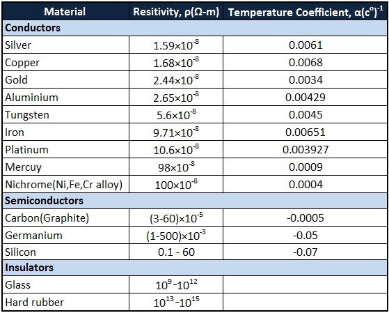
For various conductors, semiconductors and insulators, the resistivity values vary linearly with variations in temperature. The change in electrical resistance per degree Celsius of temperature change is called the temperature coefficient of resistance. This factor is represented by the letter “alpha” (α).
A positive temperature coefficient for a material means that its resistance increases with an increase in temperature. Pure conductors will typically have a positive temperature coefficient of resistance. A negative coefficient for a material means that its resistance decreases with an increase in temperature.
Semiconductor materials (carbon, silicon, and germanium) typically have a negative temperature coefficient of resistance. Different materials with their resistivity values and temperature coefficients are given in the table below.
Conductors
Conductors are built with low resistive materials having resistivity values in the order of micro-ohms per meter (µΩ/m). Metals with terribly low electrical resistivity of the order of 1 x ohm meters are called as conductors. These metals have a large number of free electrons.
These free electrons leave the valence layer of their parental atom and form a drift of electrons known as an electric current. Therefore, metals are superb conductors of electricity.
Metals like copper, aluminium, gold and silver and other non metals such as carbon are ancient conducting materials. Most of the metallic conductors are good conductors of electricity, having smaller resistance values and high conduction values.
Throughout the process of conduction, heat flows throughout the body. During conduction this heat flow may be considered as a loss of energy and the loss increases with increase in temperature after it reaches the room temperature i.e., 25°C.
Insulators
In distinction to conductors, insulators are made up of non-metals having resistivity values in the order of 1 x ohm meters. Non-metals have only a few or no free electrons flowing through it or within the parental atomic structure as the outermost electrons are tightly bonded in covalent bonds between a pair of atoms. Since the electrons are negatively charged, the free electrons within the valence layer are easily attracted by the positively charged particles within the nucleus.
Since there are no free electrons, when a positive potential is applied, there will be no electrical current to flow through the material giving insulating properties. Therefore insulators (non-metals) are very poor conductors of electricity.
Non-metals like glass, plastic, rubber, wood, sand, quartz and Teflon are sensible examples of insulators. Glass insulators are used for prime voltage power transmission. Insulators are used as protectors of warmth, sound and electricity.
Semiconductors
Semiconductors have the electrical properties in between insulators and conductors. Smart examples of perfect semiconductors are silicon (Si), germanium (Ge) and gallium arsenide (GaAs). These elements have only a few electrons within the parental atomic structure that form a crystal lattice.
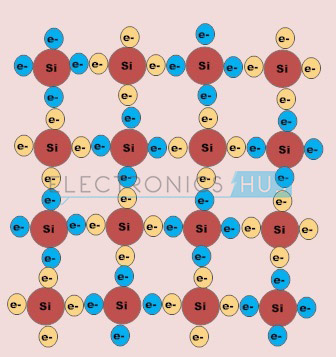
Silicon, the basic semiconductor material, contains four valence electrons within the outer shell forming four strong covalent bonds with four adjacent silicon atoms, such that each atom shares an electron with the neighbouring atom creating a strong covalent bond. The silicon atoms are organized in a lattice form, creating them a crystalline structure.
Conducting electric current is feasible with silicon semiconductor crystal by supplying external potential to the semiconductor and incorporating the impurity dopants into the semiconductor crystal thereby creating positive and negative charged holes.
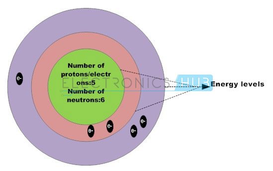
Structure of Pure Silicon Atom
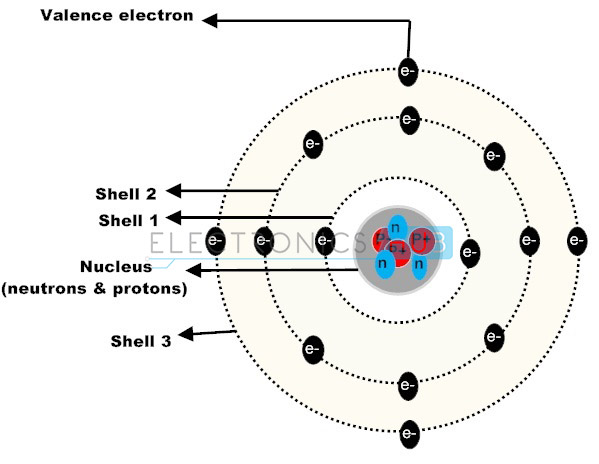
The silicon atom has 14 electrons; however the orbital arrangement has solely 4 valence electrons to be shared by alternative atoms. These valence electrons play a crucial role in photo voltaic effect. Large number of silicon atoms bond together to make a crystalline structure.
In this structure, each silicon atom shares one of its four valence electrons with their neighboring silicon atoms. The solid silicon crystal composed of a regular series of units of five silicon atoms. This regular and fixed arrangement of silicon atoms are unit is referred to as a crystal lattice.
N-Type Semiconductor
Impurities like phosphorous, arsenic and antimony are added to the silicon crystalline structure, to transform intrinsic semiconductor into extrinsic semiconductor. These impurity atoms are known as pentavalent impurities as a result of the five valence electrons in the outermost shell to share the free electrons with the neighbouring atoms.
Pentavalent impurity atoms are also known as donors because the five valence electrons in the impurity atom bond with the four valence electrons of silicon forming four covalent bonds, leaving one free electron. Each impurity atom produces a free electron within the conduction band. Once a positive potential is applied to the N-type semiconductor, the remaining free electrons form a drift to produce an electrical current.

An N-type semiconductor is a better conductor than the intrinsic semiconductor material. The majority charge carriers in N-type semiconductors are electrons and minority charge carriers are holes. The N-type semiconductors are not negatively charged, because the negative charge of donor impurity atoms is balanced by the positive charge within the nucleus.
The major contribution to the electric current flow is negatively charged electrons though there is some amount of contribution by the positively charged holes due to electron-hole pair.
N-type Semiconductor Doping
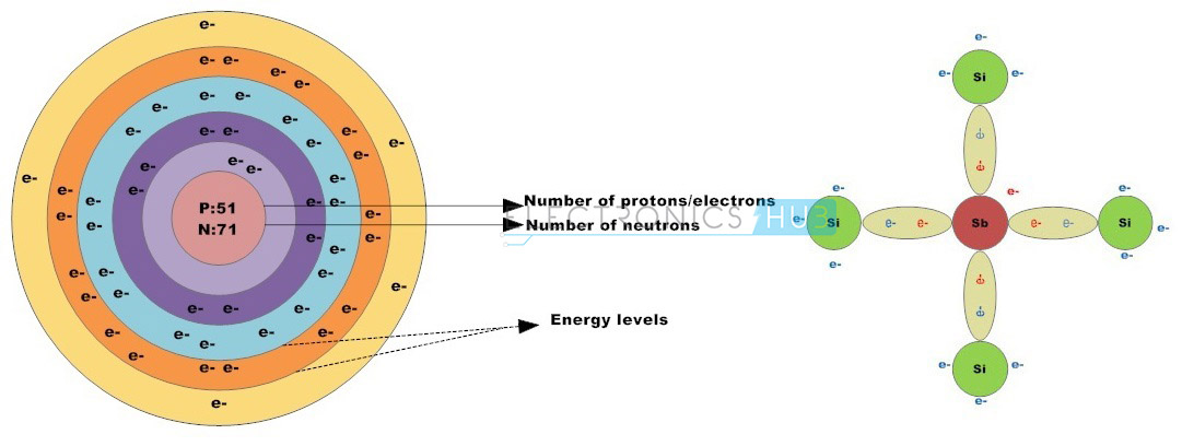
If group 5 element, such as Antimony impurity is added to the silicon crystal, the Antimony atom builds four covalent bonds with four silicon atoms by bonding the valence electrons of antimony with the valence electrons within the silicon outermost shell, leaving one free electron. Therefore the impurity atom has donated a free electron to the structure so these impurities are referred to as donor atoms.
P-Type Semiconductor
The group 3 elements such as boron, aluminium and indium are supplementary to the silicon crystalline structure having solely three electrons within the outermost shell, form three closed covalent bonds, leaving the hole in the covalent bond structure and therefore a hole in the valence band of the energy level diagram.
This action leaves an abundant number of positively charged carriers referred to as holes in the crystalline structure when there is electron deficiency. These group 3 elements are called as trivalent impurity atoms.
The presence of abundant holes attracts the neighboring electrons to sit in it. As long as the electron fills the holes in the silicon crystal there will be new holes behind the electron as it goes far from it. The newly created holes successfully attract the electrons, creating other new holes leads to the movement of holes, creating a standard electric current flow in the semiconductor.
The movement of holes in the silicon crystal seems the silicon crystal as a positive pole. As long as the impurity atoms invariably generate holes, group 3 elements are referred to as acceptors as a result of the impurity atoms are continually accepting the free electrons.
The doping of group 3 elements in silicon crystal leads to P-type semiconductor. In this P-type semiconductor holes are the majority charge carriers and electrons are the minority charge carriers.
P-Type Semiconductor Doping
If group 3 elements such as such as boron, gallium and indium are added to the semiconductor crystal, the impurity atoms having three valence electrons form three strong covalent bonds with the silicon crystal valence electrons leaving one vacancy. This vacancy is called as a hole and it is diagrammatically represented by a small circle or positive sign due to the absence of a negative charge.
Semiconductor Basics Summary
N-type materials are type of materials formed by adding group 5 elements (pentavalent impurity atoms) to the semiconductor crystals and conduct the electric current by movement of electrons.
In N-type Semiconductors
- The impurity atoms are pentavalent elements.
- Impurity elements with solid crystal give a large number of free electrons.
- Pentavalent impurities are also called as donors.
- Doping gives the less number of holes in relation to the number of free electrons.
- Doping with group 5 elements results in positively charged donors and negatively charged free electrons.
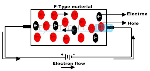
P-type materials are a type of materials formed when group 3 elements (trivalent impurity atoms) are added to the solid crystal. In these semiconductors the current flow is mainly due to the holes.
In P-type Semiconductors
- The impurity atoms are trivalent elements.
- Trivalent elements results in excess number of holes which always accepts electrons. Hence trivalent impurities are called as acceptors.
- Doping gives the less number of free electrons in relation to the number of holes.
- Doping results in negatively charged acceptors and positively charged holes
Both p-type and N-type are electrically neural on their own because the contribution of electrons and holes required for conducting electrical current are equal due to electron-hole pair. Both boron (B) and antimony (Sb) are called metalloids because they are the most commonly used doping agents for the intrinsic semiconductor to improve the properties of conductivity.

3 Responses
“Diodes are the foremost active components” Is it right?
For p type semiconductor which group element is used (15th or 13th)
Please help
Doping of groups 14 elements with group 13 elements (such as Indium) produces holes (electron deficiency) in the crystals. Thus, p-type semiconductors are produced.