A solder mask is a crucial element in the manufacturing of printed circuit boards (PCBs), often overlooked but essential for ensuring the reliability and performance of electronic devices. This protective layer, applied to the surface of the PCB, serves multiple functions that go beyond just giving the board its characteristic green color. In this blog post, we’ll explore what a solder mask is, its types, and how it contributes to the overall durability and functionality of electronic components.
What Is Solder Mask?
Solder mask, also known as Solder resist, is an integral component in electronic manufacturing. It is essentially a thin layer of protective coating applied to printed circuit boards (PCBs) to cover everything on the board (copper traces) except the solder pads. Without solder mask, when the board (or rather the copper traces on the board) reacts with atmosphere, it loses its chemical properties and also starts to rust due to oxidation. The solder mask prevents the board from reacting with oxygen. Besides, contamination such as dust and debris may get settled on the board which can lead to electrical shorts.
The solder mask shields the copper traces on the PCB surface from environmental factors and inadvertent electrical connections during soldering. It acts as a barrier, preventing solder from bridging adjacent conductive areas on the board. This shielding property is crucial for ensuring the reliability and functionality of electronic devices. Without solder mask, the risk of short circuits and electrical malfunctions significantly increases during the assembly process and throughout the operational life of the device.
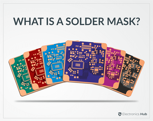
The traditional green color coating that you see on the PCBs is the solder mask. Nowadays, PCBs come with different colored solder masks. Resin is the major ingredient in a solder mask because it offers good resistance against humidity and temperatures. On top of this, it does not conduct electricity.
We can coat both the top side and bottom side of the PCB with solder mask. In some cases, the top side will have one color and the bottom side will have a different color. Arduino Uno board is a classic example of this.
What Is The Purpose Of A Solder Mask?
Solder mask serves a multifaceted purpose in electronic manufacturing, with its primary function being the protection of copper traces on printed circuit boards (PCBs). These delicate pathways carry electrical signals throughout the device, making their preservation critical to overall performance. By shielding the copper traces from environmental factors such as moisture, dust, and oxidation, solder mask prolongs the lifespan of the PCB and ensures long-term reliability.
It also plays a crucial role in preventing solder bridging during the assembly process. When solder flows uncontrollably, it can inadvertently connect adjacent conductive areas on the PCB, leading to short circuits and malfunctions. Solder mask acts as a barrier, confining solder to designated solder pads and preventing it from spreading to unintended areas. This precise control over solder application enhances the integrity of the electrical connections and reduces the risk of defects in the final product.
Additionally, solder mask provides insulation for conductive areas on the PCB, particularly those that should not come into direct contact with solder. By covering non-solderable regions such as component mounting areas, solder mask ensures that only the intended conductive surfaces are exposed during the soldering process. This insulation property not only facilitates efficient soldering but also minimizes the potential for electrical shorts or signal interference within the device.
The purpose of solder mask encompasses protection, prevention, and insulation, all of which are essential for achieving reliable and high-quality PCB assemblies.
Importance Of Solder Mask In Electronic Manufacturing
In electronic manufacturing, the application of solder masks is indispensable for several reasons. Firstly, it safeguards the delicate copper traces that form the intricate pathways for electrical signals on the PCB. Without this protection, the copper traces are vulnerable to corrosion, oxidation, and physical damage from handling or environmental exposure.
Moreover, the solder mask plays a pivotal role in facilitating the soldering process during PCB assembly. By covering non-solderable areas and exposing only the designated solder pads, it ensures precise and reliable solder joints between electronic components and the PCB. This not only enhances the mechanical strength of the connections but also mitigates the risk of solder bridges or shorts, which can compromise the functionality and lifespan of the electronic device.
Types Of Solder Masks
PCBs come with different types of solder masks. Irrespective of the type, they all undergo a process of thermal cure after the pattern is defined. Below are the different types of solder masks,
1. Top And Bottom Side Masks
When you look at other PCB solder mask guides, you’ll find two more types: top-side and bottom-side masks. These terms simply refer to the solder masks on the top and bottom sides of the PCB. They don’t relate to any specific fabrication method or material.
2. Epoxy Liquid
Epoxy-based solder masks are one of the most commonly used types, valued for their affordability, versatility and compatibility with diverse PCB substrates. These masks offer robust protection for copper traces and exhibit good thermal and chemical resistance, making them suitable for a wide range of applications. The solder mask is silk-screened through a pattern and is coated over the PCBs.
3. Liquid Photoimageable Solder Mask
Liquid Photoimageable Solder Mask (LPI) is another prominent solder mask technology known for its exceptional resolution and precise patterning capabilities. LPI solder masks are applied in liquid form and cured using ultraviolet (UV) light, allowing for intricate designs and fine features on the PCB surface. This type of solder mask is favored for high-density PCBs and applications requiring precise alignment and registration.
4. Dry Film Solder Mask
Unlike liquid solder masks, Dry Film Solder Mask (DFSM) is applied as a dry film, which is laminated onto the PCB surface and then photolithographically patterned. This method ensures consistent coverage and thickness, making DFSM ideal for applications requiring strict dimensional control and uniform insulation properties. Dry Film Solder Mask stands out for its uniform thickness and excellent dielectric properties.
Solder Mask Application Process
There is a common misconception that applying a solder mask is simple and you can do it yourself. It is not entirely true. The DIY solder masks will only work on simple PCBs. Besides, you have to be aware of the current trends, use correct equipment and manufacturing processes to apply reliable solder masks. The application of solder mask onto printed circuit boards (PCBs) involves several sequential steps, each crucial to achieving optimal performance and reliability. Below are the steps you have to follow while applying solder masks.
Step 1: Cleaning The Board
It begins with the preparation of the PCB surface, where cleanliness and surface quality are paramount. Any dust, contaminants, or residues must be thoroughly removed through cleaning and surface treatment processes to ensure proper adhesion and uniform coverage of the solder mask. Besides, the board should be dry.
Step 2: Ink Coating The Solder Mask
Once the PCB surface is prepared, various application methods can be employed to deposit the solder mask material onto the substrate. Screen printing, a commonly used method, involves transferring solder mask ink through a stencil onto the PCB surface using a squeegee. This technique offers high throughput and can accommodate large-scale production runs.
Alternatively, curtain coating involves pouring solder mask material onto the PCB surface through a moving curtain of liquid, ensuring even coverage and thickness. Inkjet printing, a newer method gaining popularity, utilizes precision printing technology to deposit solder mask material layer by layer, offering flexibility and customization options for intricate designs. You have to decide the thickness of the solder mask by considering the number of electronic components, reliability demand, and board thickness.
Step 3: Pre-hardening
The main purpose of this process is to ensure the solder mask coating is solid on the board and remove the excessive coating.
Step 4: Imaging And Hardening
Following the application of solder mask, the curing or development process is initiated to transform the liquid or semi-solid material into its final solid state. This step is crucial for achieving the desired properties of the solder mask, including adhesion, hardness, and chemical resistance.
The process involves covering the board with a transparent film that has circuit images. Then, depending on the type of solder mask used, curing may involve exposure to heat, ultraviolet (UV) light, or other energy sources to initiate cross-linking or polymerization reactions. The part of the board that is not covered by the circuit images of the transparent film will become hard. The part covered by the circuit images still remains in the pre-hardening state. Proper control of curing parameters such as temperature, time, and intensity is essential to ensure uniformity and consistency across the PCB surface.
Now, put the board into a developer to clean the excessive solder mask. This will clearly expose the parts with solder pads.
Step 5: Hardening And Cleaning
Once again harden the board so that the ink coating becomes hard on the board surface. Then, clean the board to remove any dust particles from its surface. After this, you can smoothen the surface and assemble the electronic components.
Factors To Consider When Choosing A Solder Mask
When choosing a solder mask for your PCB (Printed Circuit Board) projects, it’s important to consider several factors to ensure it fits your design needs. Here’s a simplified guide:
- Color And Visibility: The color of the solder mask affects how easily you can see traces and components. Common colors are green, red, blue, and black. Pick a color that provides a good contrast with your solder and components.
- Material Compatibility: The solder mask material should work well with your PCB’s base material, solder, and surface finish. Common materials include epoxy liquid, dry film, and top coating, which offer protection against solder or plating.
- Resolution And Alignment: Ensure the solder mask’s resolution matches your PCB’s design density. High-resolution masks are crucial for boards with fine pitch components to avoid bridges and ensure accuracy.
- Thermal Properties: The solder mask should withstand high temperatures if your PCB will be exposed to heat. It should resist heat and maintain adhesion under thermal stress.
- Chemical Resistance: The solder mask should resist chemicals used during manufacturing and cleaning, including solvents and cleaning agents.
- Durability And Reliability: A good solder mask protects copper traces from oxidation and physical damage. It should withstand handling during assembly and use.
- Curing And Processing Time: Different solder masks require different curing processes, like UV or thermal curing. Consider your production capabilities and timeline when choosing a mask.
- Cost And Availability: Consider the cost and availability of the solder mask, especially if you’re working on a large-scale project.
- Environmental Considerations: If sustainability is a priority, choose solder masks made with environmentally friendly materials and processes.
By considering these factors, you can select a solder mask that meets the specific needs of your PCB design and manufacturing process.
What Are The Most Important Functions Of Solder Mask?
Solder masks, or solder resistors, are vital in the production and performance of printed circuit boards (PCBs). Here’s a simplified look at its key functions:
- Isolation: The solder mask provides electrical isolation on the PCB. It covers non-conductive areas, leaving only the necessary pads exposed for soldering. This prevents accidental shorts between closely spaced conductive traces.
- Corrosion Protection: The solder mask shields the copper circuits from moisture, dust, and chemicals, which can cause corrosion. This protection helps the PCB last longer by keeping its electrical connections intact.
- Visual Appearance: The solder mask also enhances the PCB’s look, giving it a uniform, professional finish. It can be used to distinguish different product versions or match the branding of the device.
- Markings – Labels: Solder masks can include labels like component identifiers, polarity markings, and logos. These markings are useful during assembly and provide important information to manufacturers and users.
- Component Holes: The solder mask is applied precisely to avoid covering holes for components that need to be soldered. This precision is crucial for parts like through-hole components and connectors.
- Edge Coverage: The edges of a PCB are vulnerable to damage and corrosion. Covering the edges with a solder mask helps protect these areas, enhancing the board’s durability.
- Number Of Layers Of Solder Mask: The number of solder mask layers can vary. More layers might be used to provide extra protection in harsh environments or to meet strict industry standards, particularly in sectors like aerospace and healthcare.
Each of these functions ensures the PCB’s reliability and performance, highlighting the critical role of solder masks in PCB design and manufacturing.
Solder Mask Design Tips
It is possible to design a PCB without the solder mask. But the solder mask makes the PCB reliable and increases the lifetime by preventing oxidation and preventing solder bridges and gives the PCB a clean and professional look.
Using any latest PCB software, you can create an automated solder mask. Before designing the board, contact the board manufacturer to check the size and thickness of the board. Besides, you have to understand the spacing that you can give between copper pads.
The most common reasons for PCB failure are due to excessive solder mask openings, insufficient openings, and a mismatch between the number of openings and copper pads.
To prevent this from happening, you have to take extra precautions while making the design of the solder masks with circuit components. Take extra care during the design file modification and confirm the design matches with the requirements of the electronic components.
Frequently Asked Questions
Yes, it is possible to make a PCB without solder masks. But, coating a solder mask prevents oxidation and solder bridges from forming due to closely placed copper pads. This ensures reliability and a longer lifetime of the PCB.
Solder mask openings are the parts of the PCB that are not covered by the solder mask. In these places, copper pads are fitted. Then, solder paste is applied to these pads to assemble electronic components.
Solder mask clearance is the space between two copper pads. The solder mask clearance should be more to prevent the formation of solder bridges. A solder bridge is the unintentional connection of two electronic components in a PCB.
Green is the most common color used on PCBs. Because green color provides good visibility of the electronic components. Red and blue are the other common colors. Some boards have one color on the top surface and another color on the bottom surface.
Solder paste is applied on the copper pads, that is the part not covered by the solder mask. The paste helps in the soldering of electronic components on the PCB surface.
Conclusion
We cannot overstate the significance of solder mask in electronic manufacturing. In this guide, we’ve uncovered its pivotal role in protecting copper traces, preventing solder bridging, and insulating conductive areas on printed circuit boards (PCBs). By serving as a barrier against environmental factors and inadvertent electrical connections, solder mask ensures the reliability, longevity, and performance of electronic devices. Its application process involves surface preparation, various deposition methods, and curing techniques to achieve high-quality PCB assemblies.
While solder masks can be prepared and coated over PCBs at home, you need to use the right tools and manufacturing techniques. You need to decide the thickness of the solder mask and understand how many electronic components you are integrating on the PCB. Besides, position the transparent circuit images layer over the board accurately and leave enough space between the copper pads is very critical.
If you have any further queries or doubts, you can let us know using the comments section. We will help you out. You can also post your thoughts and opinions in the comments box.
