PWM or Pulse Width Modulation is a technique that modulates the width of a rectangular pulse wave in order to get a variation in the average value of the resulting wave. This method is used to encode the data corresponding to the width of the pulse with in the fixed frequency. But the main application of PWM is to control the power delivered to the loads. The power is controlled by switching the voltage between the supply and load at an extremely high rate (or depending on the load).
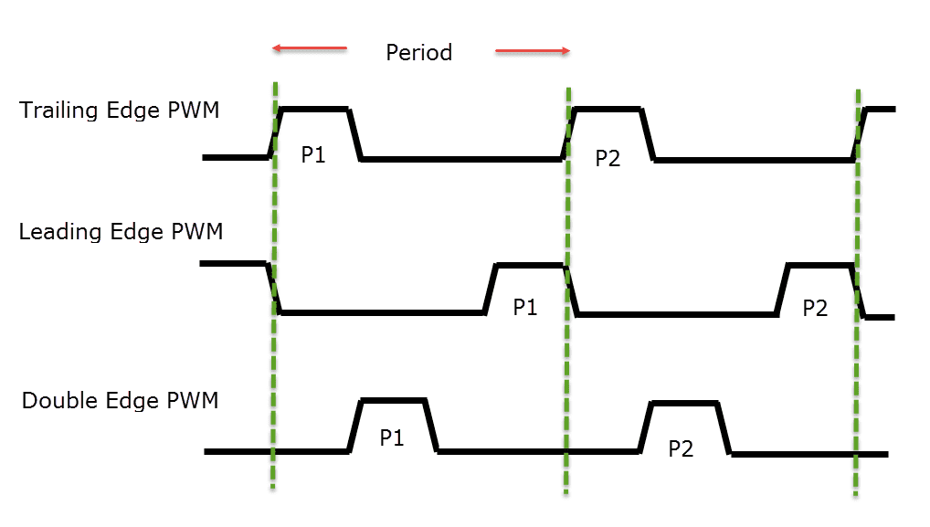
Although the PWM pin on the LPC214x series of MCUs are mentioned separately, it is based on the standard Timer block. PWM in LPC2148 are classified in to 2 types: Single Edged PWM signal and Double Edged PWM signal. In case of Single Edged PWM, the pulse will be always at the beginning or the ending of the period. Based on the position of the edge, the single edged PWM is again divided in to Trailing Edge PWM and Leading Edge PWM.
In case of Trailing Edge PWM, the pulse is fixed at the beginning of the period while the position of the trailing edge is varied. In case of Leading Edge PWM, the pulse is fixed at the end of the period and the position of the leading edge is varied.
Coming to the Double Edge PWM signal, the pulse can be placed anywhere in the period and either the leading edge or the trailing edge can be modulated.
LPC2148 has a six channel PWM block based on seven match registers that is capable of generating six channels of Single Edged PWM signal or three channel Double Edged PWM signal. The following pins on the LPC2148 are used to generate PWM.
| Output : | PWM1 | PWM2 | PWM3 | PWM4 | PWM5 | PWM6 |
| Pin Name : | P0.0 | P0.7 | P0.1 | P0.8 | P0.21 | P0.9 |
When we are talking about PWM outputs, what we actually mean is the output of the PWM Match Registers and 6 of these match registers are pinned on the LPC2148. So, PWM1 – 6 outputs are associated with PWM Match Registers 1 – 6. The PWM Match Register 0 is not pinned to LPC2148 but is used to control the Duty Cycle or period of the PWM output.
Note: In order to select the PWM function of the Pin, we need to set the PINSEL registers. PWM 1 to 4 and PWM 6 are set using PINSEL0 register and PWM 5 is set using PINSEL1.
Understanding PWM in LPC2148
Let us consider period of the PWM signal is 8 milliseconds. With the help suitable prescale value, the PWM Timer Counter (PWM TC) is set to increment every 1 millisecond. Hence, the value in the PWM Match Register 0 i.e. PWMMR0 must be 8.
The next step is to reset the value in PWM TC whenever it reaches the value in PWMMR0 and begin a new period.
Let us assume we want to generate two PWM outputs with individual pulse widths of 3 milliseconds and 5 milliseconds. For this purpose, let us use PWM1 and PWM2 i.e. PWMMR1 and PWMMR2. As per the requirement, we need to assign PWMMR1 as 3 and PWMMR2 as 5 i.e. PWMMR1 = 3 and PWMMR2 = 5.
On the start of a new period, the PWM1 and PWM2 pins will be set to HIGH by default. When the value in the PWM TC matches with the value in PWMMR1 or PWMMR2, the corresponding pins will be set to LOW. The pins will remain LOW until the next period starts. Hence, the output of the PWM pins is a single edge PWM.
Rules for Single Edge PWM Output
NXP Semiconductors (the manufacturers of the LPC series of MCUs) laid out some rules regarding the single edge PWMs in their official user manual for the LPC214x series of MCUs.
- Unless the corresponding Match Register value is ‘0’, the outputs of all the single edge PWM pins will be HIGH at the beginning of the period.
- When the PWM TC reaches the Match Register value, corresponding PWM output will become LOW. In case the value in the PWM Match Register is higher than the period of the PWM, then the PWM will be continuously HIGH.
There are also rules for Double Edge PWM Output mentioned in the user manual.
PWM Related Registers in LPC2148
Now we will see a list of register that are associated with PWM in LPC2148.
PWM Timer Control Register (PWMTCR): PWM Timer Control Register is used to control the PWM Timer Counter. This Timer Counter is specific to the PWM block. Bit 0 in the PWMTCR register is used to enable or disable the counter in PWM block. When this bit is 1, the PWM TC and PWM Prescale Counter are enabled. When this bit is 0, both are disabled. Bit 1 is used to reset the PWM TC and PWM Prescale Counter. Bit 3 is used to enable or disable the PWM Mode.
PWM Prescale Register (PWMPR): PWM Prescale Register is used to set the resolution of the PWM outputs. The PWM TC will increment for every PWMPR + 1 PCLK cycles.
PWM Match Registers (PWMMR0 – PWMMR6): Each PWM Match Register is associated with each PWM pin i.e. PWM 1 to PWM 6 are associated with PWMMR1 to PWMMR6 respectively. The values in the PWM Match Register are compared with the value in PWM TC.
PWM Match Control Register (PWMMCR): The PWM Match Control Register is used to control the operations that can be done when the value in the PWM Match registers and PWM TC register are same. Three bits are associated with each Match Register i.e. Bit 0, Bit 1 and Bit 2 for PWMMR0, Bit 3, Bit 4 and Bit 5 for PWMMR1, etc. If we consider PWMMR0, the Bit 0 in PWMMCR is used to enable an interrupt, Bit 1 is used to reset the PWM TC and Bit 2 is used to stop the PWM TC and PWM PC.
PWM Interrupt Register (PWMIR): PWM Interrupt Register is used to identify the interrupts based on PWM Match Registers. There are 7 bits in PWMIR corresponding to 7 PWM Match Register Interrupts. When an interrupt occurs, the corresponding bit in the PWMIR register is set to HIGH. If the bit is manually set to HIGH, the interrupt is reset.
| Bit in PWMIR | Corresponding Match Register |
| Bit 0 | PWMMR0 |
| Bit 1 | PWMMR1 |
| Bit 2 | PWMMR2 |
| Bit 3 | PWMMR3 |
| Bit 8 | PWMMR4 |
| Bit 9 | PWMMR5 |
| Bit 10 | PWMMR6 |
PWM Latch Enable Register (PWMLER): When PWM Match Registers are used to generate PWM signals, the PWM Latch Enable Register is used to control its update. When the value of the PWM Match Registers are updated when the PWM is active, the values will be stored in a shadow register. When an event occurs on the PWMMR0 register, the values will be transferred to the Match Registers from the shadow register only if the corresponding bit in the PWMLER is set to 1.
PWM Control Register (PWMPCR): PWM Control Register is used to enable or disable the PWM outputs and also select the mode of PWM i.e. either single edge or double edge. Bit 2 to Bit 6 in the PWMPCR register are used to set the PWM output as either single edge or double edge for PWM2 to PWM6. Bit 9 to Bit 14 are used to enable or disable the PWM1 to PWM6 outputs respectively.
Configuring PWM in LPC2148
From the list of PWM related registers we have seen above, it is clear that configuring PWM will be similar to that of Timers in LPC2148. The additional things we need to do are enabling the PWM outputs and selecting the PWM functions of the corresponding pins. Before going in to configuring the PWM we need to calculate the resolution of the PWM using the Prescale value.
PWM block derives its clock from the Peripheral Clock (PCLK) which is clocked at 60 MHz. So, to get a time required for PCLK to run for ‘X’ clock cycles at 60 MHz is
X / (60 * 10^6).
If the Prescale is considered, then X = PR + 1. So, when we consider the Prescale value to be 59, then we get a delay of
Delay = (59 + 1) / (60 * 10^6) = 1 microsecond (1 µS).
Similarly, if we set the PR to 59999, then we get a delay of
Delay = (59999 + 1) / (60 * 10^6) = 1 millisecond (1 mS).
Now that we have seen the Prescale calculations for PWM, next we will see the steps that we need to follow in order to in initialize the PWMs.
- First thing we need to do is set the PWM function of the corresponding pins using PINSEL0 and PINSEL1 registers.
- Next, we need to select the mode of the PWM i.e. single edge or double edge using PWMPCR register. Single Edge PWM is set by default.
- The resolution of the PWM, which is defined by the Prescale value, is set to the Prescale Register.
- The cycle rate of the PWM signal i.e. the period of the PWM signal is set using the PWMMR0 register.
- The pulse widths of the PWM outputs are set using the match registers i.e. PWMMR1 through PWMMR6.
- The operations like reset of the PWM TC, interrupts etc. are set for PWMMR0 match using the PWMMCR register.
- The next important step is to set the Latch Enable bits to the corresponding Match Registers using PWMLER register.
- Next, we need to enable the PWM outputs. In order to do this, we need to use the PWMPCR register.
- Similarly, we need to reset the PWM Timers. To reset the Timers, we need to make use of PWMTCR register.
- And the last thing we need to do is to enable the PWM Timer Counters and the PWM Mode. For this, we have to use the PWMTCR register again.
Example Program for PWM in LPC2148
We will now see a real time example of PWM generation in LPC2148. In this example, we will control the power delivered to an LED i.e. the dimming operation of the LED using PWM Function. For this we assume that an LED is connected to P0.21 which provides the PWM5 output. Also, four push buttons are connected to P0.15, P0.16, P1.16 and P1.17 pins as per the development board we are using for the demonstration.
#include<lpc214x.h>
int main()
{
PINSEL0=0x00000000; // P0.0 to P0.15 pins of PORT0 as GPIO
PINSEL1=0x00000400; // P0.21 Pin of PORT0 as PWM
PINSEL2=0x00000000; // P1.16 to P1.31 pins of PORT1 as GPIO
/*Configure the PLL block and set the CCLK and PCLK at 60 MHz */
PLL0CON=0x01;
PLL0CFG=0x24;
PLL0FEED=0xaa;
PLL0FEED=0x55;
while (! (PLL0STAT & 0x00000400));
PLL0CON=0x03;
PLL0FEED=0xaa;
PLL0FEED=0x55;
VPBDIV=0x01;
/* Setup and initialize the PWM block */
PWMPCR=0x00; // Single Edge PWM Mode
PWMPR=60000-1; // Resolution of PWM is set at 1 mS
PWMMR0=10; // Period of PWM is 10 mS
PWMMR5=1; // Pulse width of PWM5 is 1 mS
PWMMCR= (1<<1); // PWMTC is reset on match with PWMMR0
PWMLER= (1<<5)| (1<<0); // Update Match Registers PWMMR0 and PWMMR5
PWMPCR= (1<<13); // Enable PWM5 output
PWMTCR= (1<<1); // Reset PWM TC and PWM PR
PWMTCR= (1<<0)| (1<<3); // Enable PWM Timer Counters and PWM Mode
while (1)
{
if (! ((IO0PIN) & (1<<15))) // Check for P0.15
{
PWMMR5 = 1;
PWMLER = (1<<5); //Update Latch Enable bit for PWMMR5
}
else if ( ! ((IO0PIN) & (1<<16))) // Check P0.16
{
PWMMR5 = 2;
PWMLER = (1<<5);
}
else if (! ((IO1PIN) & (1<<16)) ) // Check for P1.16
{
PWMMR5 = 4;
PWMLER = (1<<5);
}
else if (! ((IO1PIN) & (1<<17))) // Check for P1.17
{
PWMMR5 = 8;
PWMLER = (1<<5);
}
}
//return 0;
}
