ARM LPC2148 microcontroller is great because of its versatile GPIO (General Purpose Input/Output) ports. These ports let you control electrical signals for many uses, from blinking LEDs to talking with other devices. Knowing how to set up and use the LPC2148’s GPIOs is key for developers in embedded systems. It helps make input and output functions that fit exactly what a project needs.
What is LPC2148 and GPIO
LPC2148 is a 32-bit Microcontroller based on the ARM7TDMI-S Family. It is manufactured by NXP Semiconductors (formerly Philips) and is one of the widely used and highly successful ARM7 based Microcontroller.
Even though ARM7 family is considered obsolete with the introduction of many advanced processors and controllers, it is one of the best and easiest microcontrollers to work around for beginners in ARM based microcontrollers.
Before going in to the details of the input/output pins, we’ll see some of the key features of the LPC2148 microcontroller.
- LPC2148 is a -bit microcontroller based on ARM7 family (ARM7TDMI-S to be specific) and is available in a 64 pin LQFP Package (Low Profile Quad Flat Package).
- It has an on-chip static RAM of 32kB and an on-chip flash memory of 512kB.
- LPC2148 has an on-chip boot loader software that can be used to program the microcontroller using the feature of In-System Programming.
- It also has the feature of in-Application Programming using which the user can program the microcontroller without using the boot loader software.
- It has an embedded in-circuit emulator that helps in real time debugging.
- LPC2148 has two 10-bit ADCs (ADC0 and ADC1) of Successive Approximation type.
- It also has a 10-bit DAC of Resistor String type.
Other features can be found in the official datasheet and user manual.
General Purpose Input Output (GPIO) pins of a microcontroller are the first thing we need to learn before starting its embedded programming as input/output pins are the only way to interface with the microcontroller. GPIO pins can be used for driving loads, reading digital and analog signal, controlling external components, generating triggers for external devices etc.
LPC2148 has two IO ports namely PORT0 (P0) and PORT1 (P1). These two IO ports are of 32-bit wide and are provided by the 64 pins of the microcontroller.
The naming convention of the I/O pins on the LPC2148 Microcontroller is Pa.bc where ‘a’ is the number of the port i.e. 0 or 1 (as LPC2148 has only two ports) and ‘bc’ is the number of the pin in the port a. For example, P0.1 indicates pin number 1 of PORT0 and P1.10 indicates pin number 10 of PORT1.
PORT0 is a 32-bit wide input/output port with dedicated direction control bits for each physical pin. Out of the 32 pins, 28 pins can be used as general purpose bidirectional I/O pins. Pin P0.31 is an output only pin. Pins P0.24, P0.26 and P0.27 of PORT0 are not available.
PORT1 is also a 32-bit wide input/output port. In PORT1, pins P1.0 to P1.15 are not available and pins P1.16 to P1.31 are the available general purpose input/output pins.
Most of the pins in both the I/O ports of the LPC2148 have more than one function i.e. they are multiplexed with different functions. For example, Pin 19 of the LPC2148 has three functions namely P0.0, a general purpose I/O pin, TXD0, the transmitter O/P for UART0 and PWM1, the pulse width modulator O/P 1.
At any point of operation, each pin can have a single function and the function can be selected with the help of three Configuration Registers which control the multiplexers to allow connection between the external pin and the on-chip peripheral.
The configuration register is called PINSEL and is classified in to three registers: PINSEL0, PINSEL1 and PINSEL2. These configuration registers are of 32-bit wide. Any pin on the LPC2148 can have a maximum of 4 functions. Hence in order to select one of the four functions, two corresponding bits of the PINSEL register are needed. So, a 32-bit PINSEL register can control 16 pins with 2-bits to control each pin.
PINSEL0 controls PORT0 pins P0.0 to P0.15, PINSEL1 controls PORT0 pins P0.16 to P0.31 and PINSEL2 controls PORT1 pins P1.16 to P1.31.
The following table shows the PINSEL0 and corresponding functions on the PORT0.
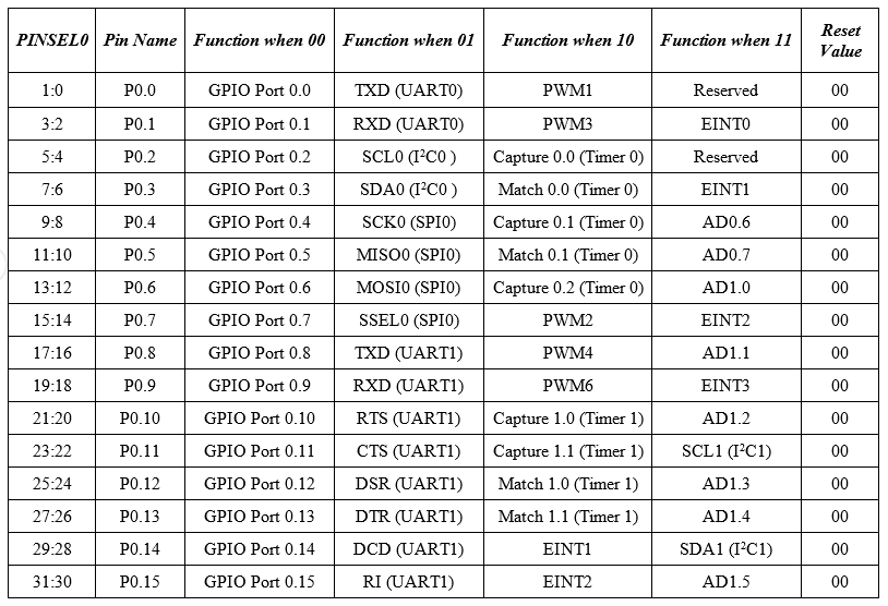
The default function of all the Pins is GPIO. But it is a good programming practice to mention “PINSEL0=0” in order to select the GPIO function of the Pins.
GPIO function is the most frequently used functionality of the microcontroller. The GPIO function in both the Ports are controlled by a set of 4 registers: IOPIN, IODIR, IOSET and IOCLR.
IOPIN: It is a GPIO Port Pin Value register and can be used to read or write values directly to the pin. The status of the Pins that are configured as GPIO can always be read from this register irrespective of the direction set on the pin (Input or Output).
The syntax for this register is IOxPIN, where ‘x’ is the port number i.e. IO0PIN for PORT0 and IO1PIN for PORT1.
IODIR: It is a GPIO Port Direction Control register and is used to set the direction i.e. either input or output of individual pins. When a bit in this register is set to ‘0’, the corresponding pin in the microcontroller is configured as Input. Similarly, when a bit is set as ‘1’, the corresponding pin is configured as Output.
The syntax for this register is IOxDIR, where ‘x’ is the port number i.e. IO0DIR for PORT0 and IO1DIR for PORT1.
IOSET: It is a GPIO Port Output Set Register and can be used to set the value of a GPIO pin that is configured as output to High (Logic 1). When a bit in the IOSET register is set to ‘1’, the corresponding pin is set to Logic 1. Setting a bit ‘0’ in this register has no effect on the pin.
The syntax for this register is IOxSET, where ‘x’ is the port number i.e. IO0SET for PORT0 and IO1SET for PORT1.
IOCLR: It is a GPIO Port Output Clear Register and can be used to set the value of a GPIO pin that is configured as output to Low (Logic 0). When a bit in the IOCLR register is set to ‘1’, the corresponding pin in the respective Port is set to Logic 0 and at the same time clears the corresponding bit in the IOSET register. Setting ‘0’ in the IOCLR has no effect on the pin.
The syntax for this register is IOxCLR, where ‘x’ is the port number i.e. IO0CLR for PORT0 and IO1CLR for PORT1.
An important note to remember is that since the LPC2148 is a 32-bit microcontroller, the length of all the registers mentioned is also 32-bits. Each bit in the above mentioned registers is directly linked to the corresponding pin in the microcontroller i.e. bit ‘a’ in IO0SET corresponds to Pin ‘a’ in the PORT0.
Registers in LPC2148 follow Big Endian format i.e. bit 0 is the LSB on the extreme right of the register and bit 31 is the MSB on the extreme left of the register.
Another important note is that when reset, all the pins are set as GPIO pins and the direction of each pin is set as Input.
Now, we’ll see how to use the above mentioned registers in programming. First, is to set the direction of a pin. For example, if we want to set 4th pin of PORT0 i.e. P0.3 as output, then it can be set in various ways as shown below.
Method 1: IO0DIR = (1<<3);
This is a direct assignment method where the binary value (1) is set directly on the pin. All the other pins are set to 0. This method should be avoided as the value is directly being assigned in the register and while P0.3 is assigned as ‘1’, all the other pins are forced to be assigned ‘0’.
An alternative to this method is ORing the register and then assigning the value. This can be done in two ways.
Method 2: IO0DIR | = 0x00000008;
In this method, the hexadecimal value of the register is assigned after ORing the register with itself. In this way, the other pins other than the desired pin (P0.3 in this case) are not affected. This method is useful if we want to assign many pins without affecting the other pins.
Method 3: IO0DIR | = (1<<3);
This is similar to the above method except that only a single pin is affected.
Other registers can also be set using the same methods. Now, we’ll see an example of setting pin 15 of PORT0 i.e. P0.15 as output and drive the pin High.
For this we need to use two registers: IODIR and IOSET.
IO0DIR | = (1<<15); // Configuring P0.15 as output.
IO0SET | = (1<<15); // Make the O/P pin P0.15 as High
We’ll see another example where pin 11 of PORT0 is set as output and the output of this pin is set to logic 1 and then to logic 0.
For this we need to use three registers: IODIR, IOSET and IOCLR.
IO0DIR | = (1<<11); // Configuring P0.11 as output.
IO0SET | = (1<<11); // Make the O/P pin P0.11 as High.
IO0CLR | = (1<<11); // Make the O/P pin P0.11 as Low.
Now, we’ll see an example where more than one pin has to be set as output and the value of that pin must be HIGH. Consider pins 7 and 14 of PORT0 (P0.7 and P0.14).
IO0DIR | = (1<<7) | (1<<14); // Configuring pins P0.7 and P0.14 as output.
IO0SET | = (1<<7) | (1<<14); // Make the O/P of pins P0.7 and P0.14 as High.
Once we have seen how to set the direction of pins, setting the pin as High or Low, now we’ll jump into real time embedded programming. Similar to “Hello, World” program in C Language, blinking an LED is the basic program in embedded system.
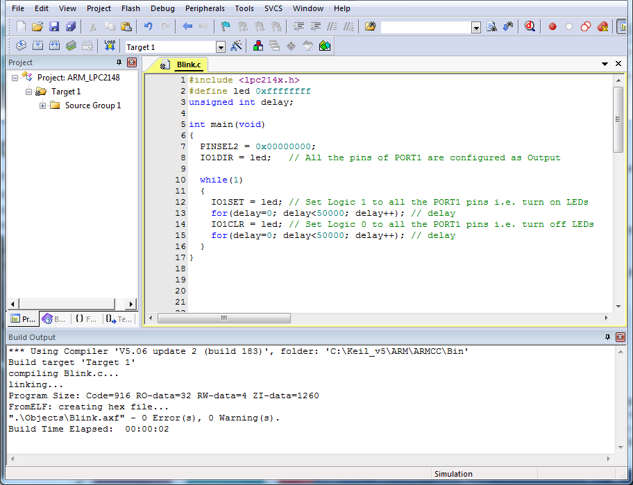
The IDE we are going to use for the development of LPC2148 based projects is Keil µVision. All the registers for LPC214X series of microcontrollers are defined in the “lpc214x.h” header file.
In this example, we’ll blink the LEDs repeatedly that are connected to PORT1 pins of the MCU.
#include <lpc214x.h>
int delay;
int main (void)
{
PINSEL2 = 0x00000000;
IO1DIR = 0xFFFFFFFF; // All the pins of PORT1 are configured as Output
while (1)
{
IO1SET = 0xFFFFFFFF; // Set Logic 1 to all the PORT1 pins i.e. turn on LEDs
for (delay = 0; delay<500000; delay++)
IO1CLR = 0xFFFFFFFF; // Set Logic 0 to all the PORT1 pins i.e. turn off LEDs
for (delay = 0; delay<500000; delay++)
}
return 0;
}
The program is self-explanatory. First, the PORT1 pins are configured as outputs using IO1DIR register. Then in an infinite loop, the pins (or LEDs connected to them) are turned ON using IO1SET register and turned OFF using IO1CLR register. A delay is introduced between the turning ON and OFF of the LEDs using a “for” loop, so that the blinking of LEDs is visible.
How to upload the program to LPC2148 Microcontroller
First, we need to install Keil Microcontroller Development Kit for ARM based microcontrollers. Then, copy and paste the code in the source code editor. Compile the code and build the code for the target i.e. LPC2148.
In order to upload the code i.e. hex file to the microcontroller, we need to use a tool called Flash Magic. Before going to upload the program, we need to confirm something about the ARM7 Development board.
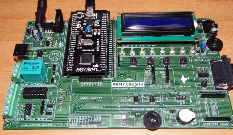
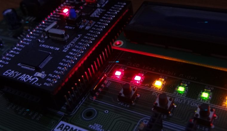
The ARM7 development board used in this series of projects has an on – board USB to Serial converter as it is shown in the following image.
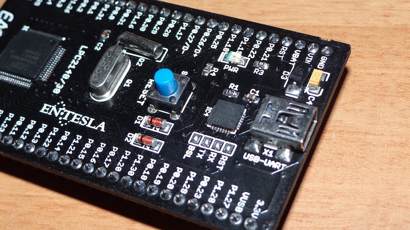
In this case, we can directly upload the program using USB connection as the LPC2148 Microcontroller has an on – chip bootloader.
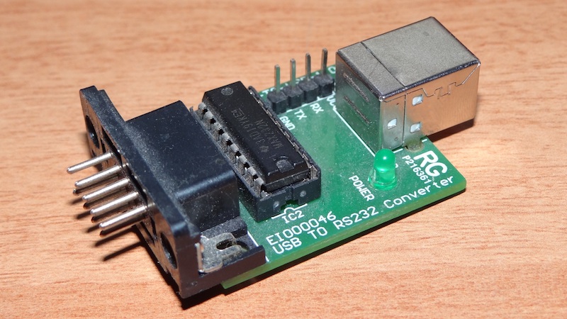
In case the ARM development board you are using doesn’t have the USB to Serial converter, then we need to use an external module as the one shown in the following image.
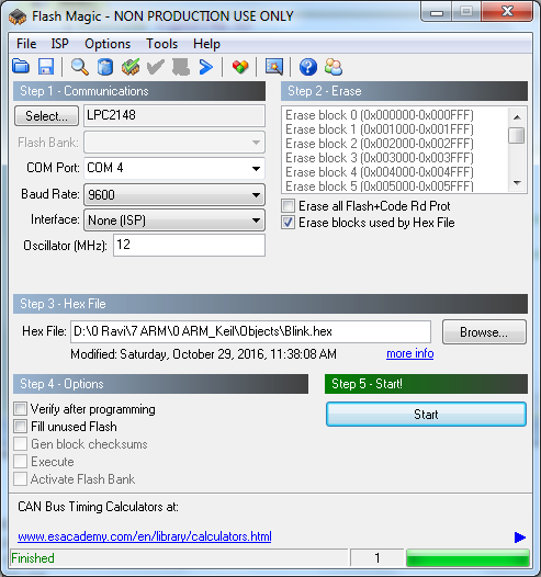
Once, we have decided the type of interface, the next step is to start the Flash Magic software and setup the appropriate COM ports. We can see the COM port in device manager in Windows. After the COM port is set, we have select the “.hex” file which is created from the Keil software after compiling and building.
Once the hex file is selected, we need to click the “Start” button and the software starts uploading the program.
If the program is uploaded successfully, we can see the output immediately on the LPC2148 development board.

One Response
Hi
How will get this ARM development board?