In this tutorial, we will see a basic introduction to ASIC, what are the different types of ASIC design techniques, the ASIC design flow, applications and many more.
In a broad sense, an Application Specific Integrated Circuit or simply an ASIC can be defined as an integrated circuit customized for a particular application or end-use rather than using it for general purpose. Some basic examples of ASICs are the IC in a DVD Player to decode the information on an optical disc or an IC designed as a Charge Controller for Lithium Ion batteries.
ASICs are quite different from other standard ICs like Microprocessors or Memories as these are designed to be used in a wide range of applications. In contrast, an ASIC can only be used in the application it was specifically designed to run.
Due to the application specific custom nature of the ASICs, they often pack more functionality at the same time being small in size, consuming less power and dissipating less heat when compared to a standard IC solution. The other main difference between standard ICs like Memories, for example and ASICs is that the designer of the ASIC can directly be the customer, who might have a clearer idea of the application.
Since the early 1980s, the world of integrated circuits has been highly influenced by ASICs. They are responsible for the expansion of the semiconductor industry, change in the business model of the integrated circuits and significant increase in IC designs and design engineers.
ASICs also influenced the whole ecosystem of the semiconductor design and manufacturing like system design, fabrication and manufacturing process, testing and packaging and the CAD tools.
A Brief History of ASICs
The origin of ASICs can be traced back to at least 20 tears before the development of Masked ROM (Read-only Memory). In the early 1970s, the concept of Gate Arrays and Standard Cells have been introduced but during the 1980s, the ASIC technology took a prominent place in the IC market throughout the World.
It is during this period that several semiconductor manufacturers and vendors, particularly from Japan, dominated the ASIC market and are regarded as ASIC Specialists.
What are the Different Types of ASIC?
The history of ASIC designs and technology can be characterized by the continuous growth and evolution of various design styles of ASIC. Statistically speaking, the CMOS based gate array style ASICs are the dominant type but there are several other types of ASIC designs.
Basically, all ASICs can be categorized into three types. They are:
- Full – Custom ASICs
- Semi – Custom ASICs
- Programmable ICs
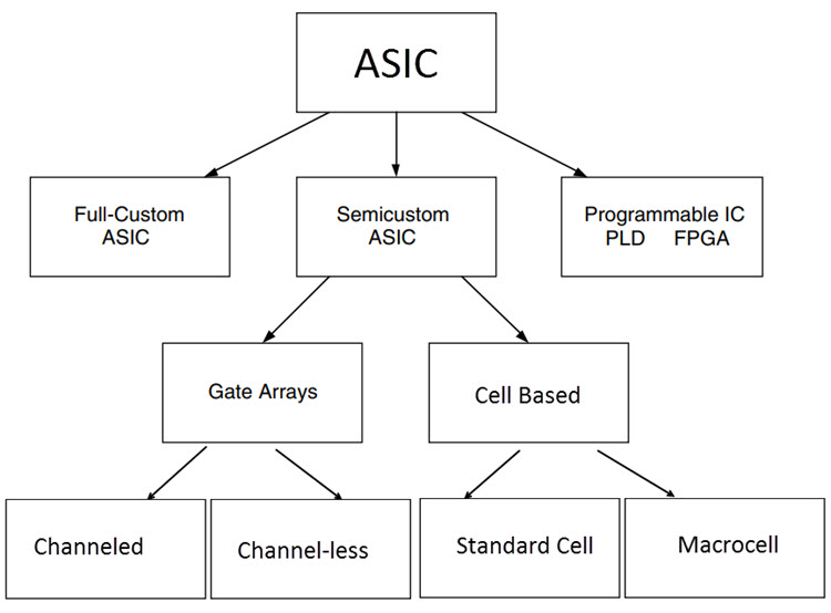
The semi-custom ASICs are again divided into Gate Array based designs and Cell based designs. Gate Arrays are further divided into Channelled and Channel-less Arrays while Cell based designs are further divided into Standard Cell and Macrocell.
Coming to Programmable ICs, all the Programmable Logic Devices like PAL, PLA, EPROM based PLD (EPLD), EEPROM based PLD (EEPLD), and field programmable devices like FPGA come under this category.
The following image shows the different types of ASIC and also the sub-categories in each type.
Let us now briefly see some of the important types of ASICs.
Full-Custom ASIC
In Full-Custom ASIC, all the logic cells, circuits and layouts are designed specifically for that particular ASIC from the ground up. The designer may choose a full-custom ASIC design only if he thinks that either the existing libraries are not fast enough or the logic cells are not small or the power consumption is high.
The main advantages of full-custom ASICs over other IC designs are it delivers the highest possible performance at the smallest possible die size. But this high performance and small size comes at a price of increased design time, complex design and overall cost of the IC itself.
Some of most common full-custom ASISs are Microprocessors, Memories, Analog Processors, Analog / Digital Communication devices, Sensors, Transducers, high-voltage ICs for Automobiles, etc.
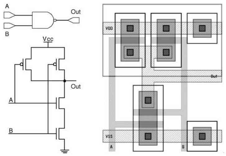
The following is a sample design of a CMOS based 2-input NAND gate, where every layer is defined.
Semi-Custom ASIC
To shorten the design time and cut down the cost of full-custom ASICs, numerous other design approaches have been developed and these are called as Semi-Custom ASIC Designs. Usually, the lowest level of hierarchy involved in semi-custom design is the logic level or gate level. This is in contrast to full-custom job, where the design and layout individual transistor might be involved.
As mentioned earlier, the semi-custom ASIS design can be further divided into Gate Arrays and Standard Cells. Let us see a little bit about these types.
Gate Array ASIC
In Gate Array based ASICs, p and n types transistors are predefined on a silicon wafer as arrays. Based on the design from the customer and the interconnections obtained from the design, the silicon vendor provides these base wafers. Therefore, the base wafer is specific to the customer as it is designed based on the customer provided connections between the transistors of the gate array.
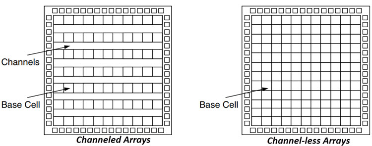
The gate arrays are again divided into two types called the Channelled Gate Array and the Channel-less Gate Array. In channelled gate arrays, the interconnections between the logic cells are performed within the predefined channels between the rows of the logic cells. In case of channel-less gate arrays, the connections are made on an upper metal layer on top of the logic cells.
Standard Cell based ASIC
A Standard Cell based ASIC uses predesigned logic cells like Gates, Multiplexers, Flip-flops, Adders etc. These logic cells are known as Standard Cells that are already designed and stored in a library. This library is imported into the CAD tool and the design can performed using the components of the library as inputs.
Typically, Standard Cell based designs are organized as rows of constant height cells on the chip, just like a row of bricks. When combined with logic-level components, standard cell-based designs can be used to implement complex functions like Multipliers and Memory Arrays.
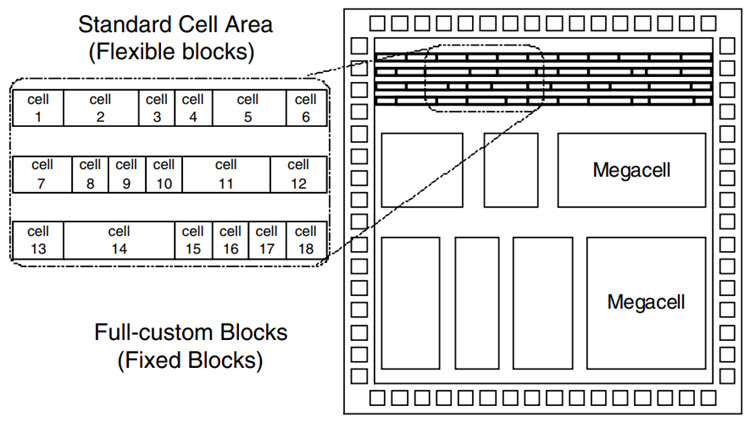
The standard cell design may also contain a larger and more complex predesigned cells like Microcontrollers or Microprocessors. These larger cells are called as Megacells.
Design Flow
Until now, you have seen a brief introduction to ASIC and also few important types of ASICs. In this section let us try to briefly understand the specific process flow and procedures involved in designing and developing an ASIC.
The following image shows a typical design flow involved in designing a semicustom ASIC. It can be basically divided into 10 steps.
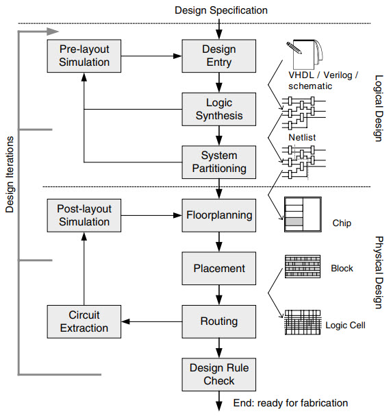
- Design Entry: In the step, the logic design is created using a Hardware Description Language (HDL) like VHDL or Verilog or with the help of Schematic entry.
- Logic Synthesis: Once the logic is designed using HDL or Schematic entry, the next step is to extract the description of the logic cells and their interconnections. This information is also called as Netlist.
- System Partitioning: The next step is to logically divide the entire system into small ASIC sized blocks.
- Pre-layout Simulation: Before going into the actual physical layout of the design, a simulation tool checks the circuit for proper working. In fact, this process is performed at every step so that if any errors are found, then it would be easy to correct them at this stage itself. The process until this step is usually regarded as Logical Design. The steps after this are related to the actual physical layout of the design.
- Floorplanning: The first step in the physical design is arrange all the blocks of the circuit on the chip.
- Placement: In this step, the location of the logic cells in a block are set.
- Routing: Once the placement of the blocks and cells is completed, then it is time to create the connections between the cells and the blocks.
- Extraction: The next step is to determine the resistance and capacitance of the interconnections previously made, since they decide the delay of the signal. Also, the delays are calculated at this stage.
- Post-layout Simulation: Once the physical design is complete, the circuit is again tested for working. The delays previously calculated are also taken into consideration for the simulation process.
- Design Rule Check (DRC): Final step is to verify the layout of the entire circuit and check whether it complies with the design rule specifications.
Applications
The area of applications of ASICs is very wide as they are basically used everywhere where there is a need for performance, customization and size. Some of the common categories of application are mentioned below.
- Sensors and Transducers
- Automotive and Avionic Components
- Satellite, Radar and related Communication processors
- Microprocessors, Memories, Microcontrollers
