In this article, we will see a special topic called Field Programmable Gate Arrays or simply FPGA. We will explore the concept of Programmable Logic Devices and different types of Field Programmable Devices (FPD) like PLA, PAL, CPLD, FPGA. Also, we will see the architecture of a typical FPGA Device along with its advantages.
Introduction
Field Programmable Gate Arrays (FPGAs) are digital ICs (Integrated Circuits) that enable the hardware design engineer to program a customized Digital Logic as per his/her requirements. The term “Field Programmable” implies that the Digital Logic of the IC is not fixed during its manufacturing (or fabrication) but rather it is programmed by the end-user (designer).
In order to provide this programmability, an FPGA consists of Configurable (or Programmable) Logic Blocks and configurable interconnects between these blocks. This configurable Logic and the Interconnections (Routing) of FPGAs makes them general purpose and flexible but at the same time, it also makes them slow and power hungry when compared to a similar calibre ASIC with Standard Cells.
It has been more than three decades since the introduction of FPGAs into the market and in this long span, they have undergone a severe technological advancement and gained a continuously growing popularity.
A Brief Note on PLD (Programmable Logic Device)
Before diving into the main topic, I want to briefly discuss the concept of Programmable Logic Devices. So, what is a PLD. It is an IC containing a large number of Logic gates and Flip-flops that can be configured by the user to implement a wide variety of functions.
The simplest of Programmable Logic Devices consists of an array of AND & OR gates and the logic of these gates and their interconnections can be configured by a programming process.
PLDs are particularly useful when an engineer wants to implement a customized logic and is restricted by the pre-configured integrated circuits. PLDs provide a way to implement a custom digital circuit through the power of hardware configuration rather than implementing it using a software.
Different Types of PLDs
Basically, PLDs can be categorized into three types. They are:
- Simple Programmable Logic Devices (SPLD)
- Complex Programmable Logic Devices (CPLD)
- Field Programmable Gate Arrays (FPGA)
The Simple Programmable Logic Devices are further divided into:
- Programmable Logic Array (PLA)
- Programmable Array Logic (PAL)
- Generic Array Logic (GAL)
Let us now see some basic details about all these PLDs.
Programmable Logic Array (PLA)
A PLA consists of an AND gate plane with programmable interconnects and an OR gate plane with programmable interconnects. The following is a simple four input – four output PLA with AND & OR gates.
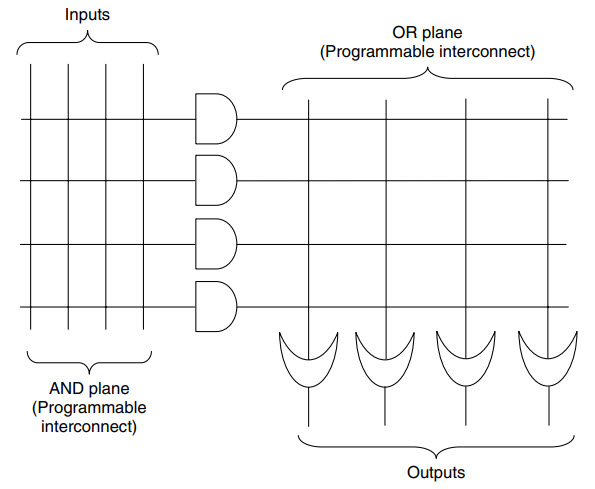
Any input can be connected to any AND gate by connecting the horizontal and vertical interconnect lines. The outputs from different AND gates can then be applied to any of the OR gates with programmable interconnects.
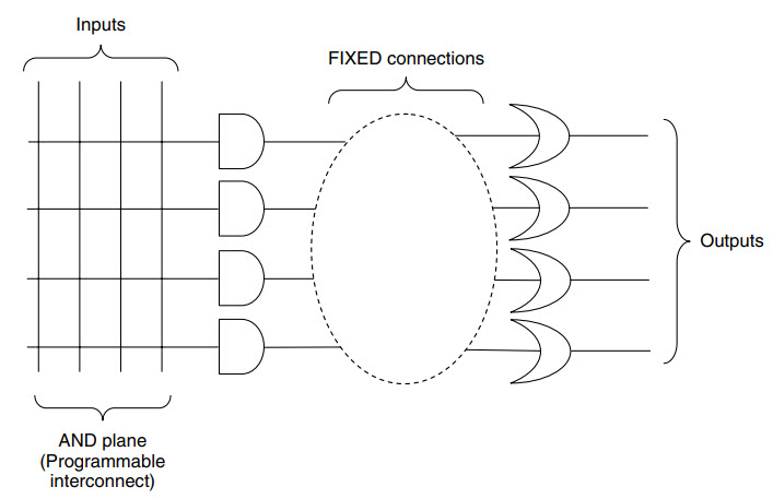
Programmable Array Logic (PAL)
A PAL is similar to the PLA but the difference is that in PAL, only the AND gate plane is programmable while the OR gate plane is fixed during fabrication. Even though PALs are less flexible than PLAs, they eliminate the time delays associated with programmable OR Gates.
Generic Array Logic (GAL)
Architecture wise, a GAL is similar to a PAL but the difference lies in programmable structure. PALs use PROM, which is one-time programmable, while GAL uses EEPROM, which can be reprogrammed.
Complex Programmable Logic Devices (CPLD)
Moving up from SPLD devices, we get CPLD. It is developed on top of SPLD devices to create mush larger and complex designs. A CPLD consists of a number logic blocks (or functional blocks), which internally consists of either a Pal or a PAL along with a Macrocell.
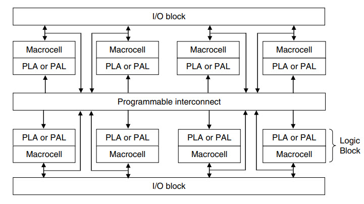
Macrocell consists of any additional circuitry and signal polarity control to provide true signal or its complement.
Field Programmable Gate Arrays (FPGA)
Complexity wise, CPLD are much more complex than SPLDs. But FPGA are even more complex than CPLDs. The architecture of an FPGA is completely different as it consists of programmable Logic Cells, programmable interconnects and programmable IO blocks.

What is an FPGA?
Field Programmable Gate Arrays or FPGAs in short are pre-fabricated Silicon devices that consists of a matrix of reconfigurable logic circuitry and programmable interconnects arranged in a two-dimensional array. The programmable Logic Cells can be configured to perform any digital function and the programmable interconnects (or switches) provide the connections among different logic cells.
Using an FPGA, you can implement any custom design by specifying the logic or function of each logic block and setting the connection of each programmable switch. Since this process of designing a custom circuit is done in the field rather than in a fab, the device is known as “Field Programmable”.
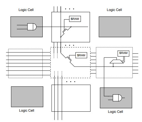
The following image shows a typical internal structure of an FPGA in a very broad sense.
As you can see, the core of the FPGA is made up of configurable logic cells and programmable interconnections. These are surrounded by a number of programmable IO blocks, which are used to talk to the external world.
Components of an FPGA
Let us now take a closer look at the structure of an FPGA. Typically, an FPGA consists of three basic components. They are:
- Programmable Logic Cells (or Logic Blocks) – responsible for implementing the core logic functions.
- Programmable Routing – responsible for connecting the Logic Blocks.
- IO Blocks – which are connected to the Logic Blocks through the routing and help to make external connections.
Logic Block
The Logic Block in Xilinx based FPGAs are called as Configurable Logic Blocks or CLB while the similar structures in Altera based FPGAs are called Logic Array Blocks or LAB. Let us use the term CLB for this discussion. A CLB is the basic component of an FPGA, which provides both the logic and storage functionalities. The basic logic block can be anything like a transistor, a NAND gate, Multiplexors, Look-up Table (LUT), a PAL like structure or even a processor. Both Xilinx and Altera use Look-up Table (LUT) based logic blocks to implement the logic as well as the storage functionalities.
A Logic Block can be made up of a single Basic Logic Element or a set of interconnected Basic Logic Elements, where a Basic Logic Element is a combination of a Look-up table (which is in turn made up of SRAM and Multiplexors) and a Flip-flop.
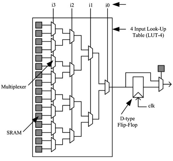
A LUT with ‘n’ inputs consists of 2n configuration bits, which are implemented by SRAM Cells. Using these 2n SRAM Bits, the LUT can be configured to implement any logical function.
Routing
If the computational functionality is provided by the Logic Blocks, then the programmable routing network is responsible for interconnection these logic blocks. The Routing Network provides interconnections between one logic block to other as well as between the logic block and the IO Block to completely implement a custom circuit.
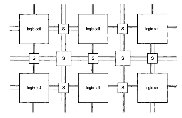
Basically, the routing network consists of connecting wires with programmable switches, which can be configured using any of the programming technologies. There are basically two types of routing architectures. They are:
- Island Style Routing (also known as Mesh Routing)
- Hierarchical Routing
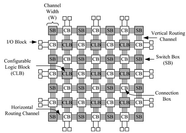
In island style routing architecture, the logic blocks are arranged in a two-dimensional array and are interconnected using a programmable routing network. This type of routing is widely used in commercial FPGAs.
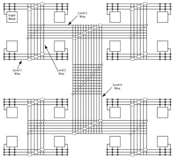
Many logic blocks are confined to a local set of connections and hierarchical routing architecture makes use of this feature by dividing the logic blocks into several groups or clusters. If the logic blocks are residing in the same cluster, then the hierarchical routing connects them in a low level of hierarchy.
If the logic blocks are residing in different clusters, then wiring is done over a higher level of hierarchy.
FPGA Programming Technologies
We have talked about the reprogrammable architecture of FPGAs quite a bit but now let us see some of the most commonly used programming techniques that is responsible for such reconfigurable architecture.
The following are three of the well-known programming technologies used in FPGAs.
- SRAM
- EEPROM / Flash
- Anti-Fuse
Other technologies include EPROM and Fusible Link but they are used in CPLDs and other PLDs but not in FPGAs, Hence, let us keep the discussion limited to FPGA related programming technologies.
SRAM
We know that there are two types of semiconductor RAM called the SRAM and DRAM. SRAM is short for Static RAM while DRAM is short for Dynamic Ram. SRAM is designed using transistors and the term static means that the value loaded on a basic SRAM Memory Cell will remain the same until deliberately changed or when the power is removed.
A typical 6 transistor SRAM Cell to store 1 bit is shown in the following image.
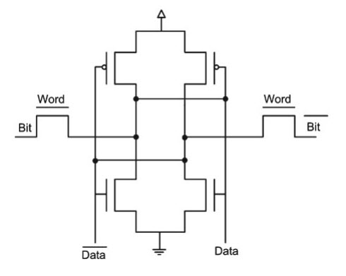
This is in contrast to the DRAM, which consists of a combination of a transistor and a capacitor. The term Dynamic refers to the fact that the value loaded in the basic DRAM Memory Cell is valid until there is charge in the capacitor. As capacitor loses its charge over time, the memory cell has to be periodically recharged to maintain the charge. This is also known as refreshing.
Many FPGA vendors implement Static Memory Cells in SRAM based FPGAs for programming. SRAM based FPGAs are used to program both the logic cells and the interconnects and they have become quite predominant due to their re-programmability and use of CMOS technology, which is known for its low dynamic power consumption, high speed and tighter integration.
EEPROM / Flash
A close alternative to SRAM based programming technology is based on EEPROM or Flash programming technologies. The main advantage of flash-based programming is its non-volatile nature. Even though flash supports re-programmability, the number of times this can be done is very small when compared to an SRAM technology.
Anti-Fuse
The anti-fuse programming technology is an old technique of producing one-time programmable devices. They are implemented using a link called the antifuse, which in its unprogrammed state has a very high resistance and can be considered an open circuit.
When programming, a high voltage and current is supplied to the input. As a result, the antifuse, which is initially in the form of amorphous silicon (basically an insulator with very high resistance) linking two metal tracks, comes to life by converting to a conducting polysilicon.
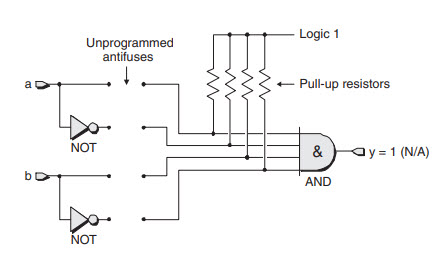
When compared to the other two technologies, the antifuse one occupies the least amount of space but comes only as one-time programmable option.
Applications
- In the early years of the introduction of the FPGAs, they were typically used to implement small to medium complex state machines and data processing tasks on small data. As their complexity and capability increased over the years, they have been incorporated in several automotive, consumer and industrial applications.
- Initially, FPGAs provided an easy option to prototype ASIC designs as they can be easily reconfigured to test and try several variations of the hardware before finalizing the main design. But their capability to function as an end-product with relatively short time-to-market and small implementation costs, they have been implemented as direct competitors to some ASICs.
- Modern FPGAs with multipliers, complex routing and on-chip RAM can facilitate DSP operations which were previously possible on dedicated Digital Signal Processors.
- With the cost of FPGAs coming down, they are getting serious contenders of embedded control applications. An FPGA can be used to implement a soft-core processor of any microcontroller along with custom IO capabilities.
