In this tutorial, we will learn about an important semiconductor component called DIAC. We will learn about its symbol, construction, working, V-I Characteristics, Applications and some example circuits.
A DIAC is much similar to the transistor so more strictly it is called as a transistor than a thyristor. However, it has an important role in Triac triggering and other thryristor based circuits. Several gate triggering circuits use this device for achieving greater triggering stability and noise immunity.
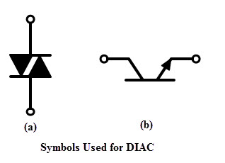
The DIAC stands for the DIode AC switch. It is a two terminal bidirectional switching device. These terminals are not named as anode and cathode in case of normal diode. This indicates that this device can be used in either direction.
Symbols of the DIAC are shown in the following image. It has two arrows in both directions, which means that it conduct for either polarity of the supply voltage. A DIAC doesn’t have a controlling terminal as a gate in case of thyristor devices.
DIAC Construction
The construction of diac is looks like a transistor; however, there are several differences between these two. Some of these are
• The doping concentrations in all the layers are identical, whereas the transistor has a highly doped emitter, lightly doped collector and moderately doped base.
• Transistor is a three terminal device, whereas the diac is a two terminal device.
• The three regions in diac are equal in size.
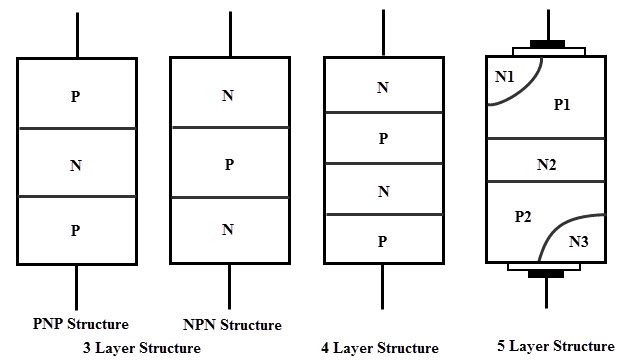
The diac can be fabricated into three, four or five layer structure. A three layer structure is more commonly used than other structure. The three layer diac can be constructed in either PNP or NPN structure. In PNP form, two terminals are connected to the outer silicon P-regions separated by N region. This structure is same as PNP transistor with no base connection.
Consider the PNP crystal structure, in which terminals 1 and 2 are connected to the P1 and P2 outer layers respectively which are separated by N layer. When the terminal T1 is positive with respect to terminal 2, junction P1- N is forward biased and P2-N is reverse biased. When the breakover voltage of P2-N is reached, the entire structure comes into the conduction mode and hence diac conducts from terminal 1 to terminal 2. The reverse will happen if terminal 2 is positive with respect to terminal 1.
Working of DIAC
As soon as the supply voltage whether positive or negative is applied across the terminals of a diac, only a small leakage current flows through the device. So the device operates in either forward or reverse blocking modes. When the applied voltage is increased to a value such that it is equal to the breakover voltage, an avalanche breakdown occurs at the reverse biased junction.
Then, it starts conducting and exhibits negative resistance characteristics, i.e., the current increases with decreasing values of applied voltage. The voltage drop during the conduction is very less and is equal to the ON state drop of the diac. The current flow increases quickly when it comes into the conduction mode. Therefore, for a safe operating level of this conduction current in either direction, a resistance is connected in series with the diac.
V-I Characteristics of DIAC
The figure below shows the V-I characteristics of DIAC which indicates the current flow through the diac with respect to the voltage across it. As long as the voltage across it is within its breakover limits that is from –VBO to +VBO, the resistance offered by the diac is very high.
So, a small leakage current flows through the device for applying positive voltage which is less than +VBO and negative voltage less than –VBO as shown in figure. The region OA in the portion of the characteristics is the blocking region. Under these conditions diac operates as an open switch. The voltages +VBO and –VBO are the breakdown voltages which are generally in the range of 30 to 50 volts.
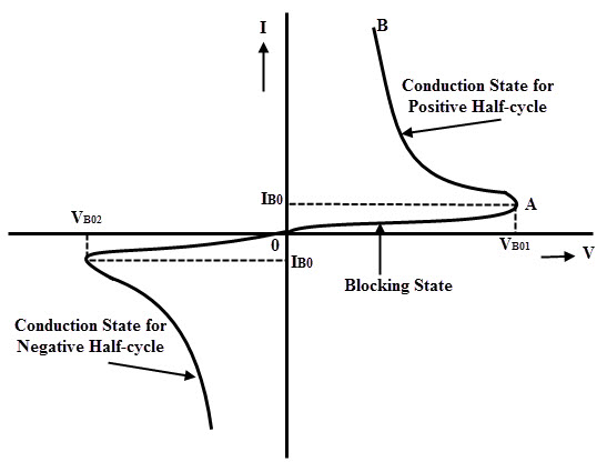
Once the positive or negative applied voltage is more than the respective breakdown voltages that means at point A in the above figure the diac begins to conduct and the voltage drop across the device becomes few volts. The portion AB represents the conduction of diac.
This conduction continuous until the device current falls below its holding current level. From the figure it is noted that the holding current and breakover voltage values are identical for reverse and forward region of operation. The first and third quadrant characteristics represent the forward and reverse bias conditions of the diac.
Applications
Since the triac requires either positive or negative gate pulse to come into the conduction state. Although it can be triggered by a simple resistance firing circuit, for a reliable and faster turn ON, a diac is used in series with the gate.
Hence the diac is mainly used as a trigger device to the triac. In today’s market, there are several Diac-Triac matched pairs are available for different control circuits. The diac is used as a trigger device in phase control circuits of motor speed control, light dimmers, heat control, etc.
Example Circuits
Light Dimmer Circuit
The figure below shows the light dimmer circuit. By using this, power fed to the lamp is controlled smoothly. The variable gate voltage is produced by RC arrangement at the gate terminal of triac. When the device is switched OFF, the rate of rise of voltage is limited by the series R4-C1 network across the triac.
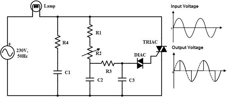
As the input voltage is applied to the circuit, c1 and c2 starts charging at a rate determined by the resistance R2. Whenever the voltage across the capacitor c3 exceeds the breakover voltage of the diac, diac triggered and starts conducting. Then, the capacitor C3 starts discharging through the conducting diac into the gate of the triac.
Therefore, the triac is turned ON and passes the current to the lamp. By varying the resistance R2, rate of charge in the capacitor is varied and hence the voltage at which the triac is triggered in both positive and negative half cycles of the input is controlled.
In above figure both supply and load voltages are shown. The firing angle of the triac can be varied up to the 180 degrees. And hence load voltage is controlled from zero value to full RMS value.
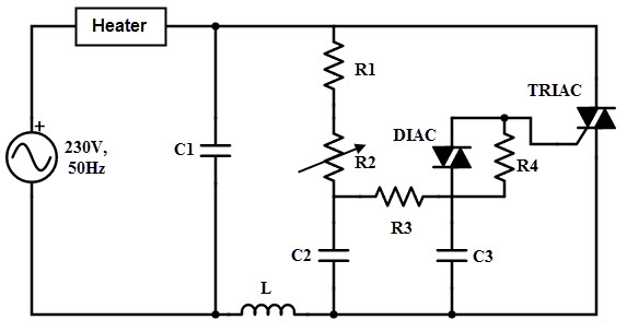
Heater Control Circuit
The figure below shows the usage of diac as a trigger device to provide a smooth control of heat produced by the heater. This circuit operation is also similar to the above circuit. The LC combination across the triac reduces the rate of rise of voltage during the turn OFF of the triac.
The positive and negative half cycle of the input voltage to the heater is controlled by adjusting the resistance R2. For all variable positions of R2 , a smooth control ensued by placing resistance R4 across the diac.

2 Responses
hello ,
I am manufacturing 650W dimmers , where the triac used in BT 12-600 , and there are 6 diac in series given to the gate terminal of triac ,
please tell me why diac are connected in series and weather number of diacs can be reduced
The concept is smooth working and any excess or shortage is adjusted.