We have already seen the circuit diagram, working and applications of 9 way Clap Switch Circuit. Now, we are going to deal another circuit named clap switch circuit for devices. I will present two circuits for clap switches, both of these circuits will be based on 555 IC and 4017 IC.
Using these circuits, you can control electrical appliances by simple clapping. Summary of the project given below:
Clap Switch Circuit Summary
- If you wish to “ON” and “OFF” the device without moving from your place, then this circuit is helpful for you.
- One more plus point of this circuit is that there is no fear of the electrical shocks as you are not required to touch any of the mechanical switches physically.
- Visual indication of the devices is also provided to you.
- With the help of this circuit, speed of the fan can also be controlled by connecting regulator with individual outputs.
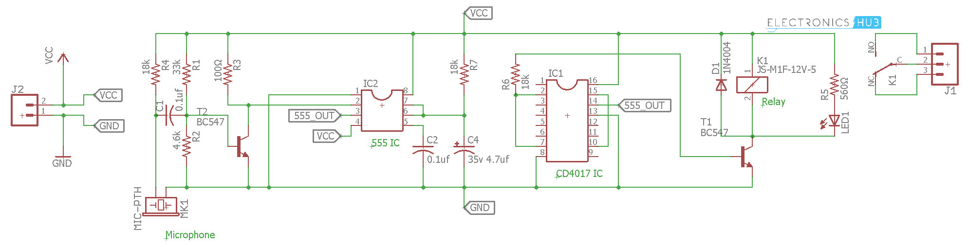
Clap Switch Circuit using 555 and 4017
In the first circuit, I will control a single relay using clap switch. When you clap once, the relay is activated and the light (or any load) is turned ON. When you clap for the second time, the relay is deactivated and the light is turned OFF.
Circuit Diagram
Components Required
- 555 IC
- CD4017 IC
- Relay
- Resistors – 100Ω, 560Ω, 4.6KΩ, 18KΩ x 3, 33KΩ
- Capacitors – 0.1µF x 2, 4.7µF
- Microphone
- BC547
- 1N4004 Diode
- LED
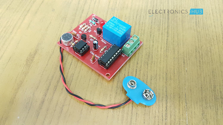
PCB for Clap Switch Circuit
I have made a simple PCB for the above mentioned clap switch circuit. The PCB layout is shown on the following image.
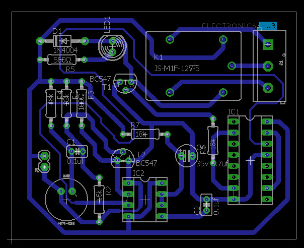
If you want to make your own PCB, I have included the Eagle CAD PCB Files. You can download them from here.
Clap Switch Circuit for Multiple Devices
In the second circuit (similar to the one above), I have added a few extra relays to control additional devices.
Circuit Diagram
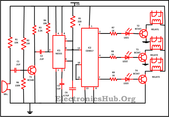
Circuit Components
- IC
- IC1(NE555) – 1
- IC2(CD4017) – 1
- Resistor
- R1,R4(10K) – 2
- R2,R7,R8,R9(1K) – 4
- R3(2.2K) – 1
- R5(220E) – 1
- R6(150) – 1
- C1,C2(.1uf) – 2
- C3(1uf) – 1
- C4(4.7uf) – 1
- Mic – 1
- LED – 3
- T1(BC548) – 1
- T2,T3,T4(BC547) – 3
- Relay – 3
Clap Switch Circuit Description
Along with some of the other components, this circuit is mainly based on the two ICs i.e. NE555 timer along with CD4017.
IC 555 timer in this circuit is wired like a monostable oscillator. For this circuit, IC NE555 monostable produces a clock pulse, which is used to give an oscillating wave at IC1 pin 3 which is an output pin. Monostable (or you can say one shot multivibrator) contains only one steady state and all we need is to trigger it externally to return it in reverse direction to its original state.
Another one is the CD4017 which is a CMOS counter/divider IC. It receives a clock signal through the clock input and in the sequential manner it turns ON all the 10 outputs, every time it gets the clock input pulse.
In order to get familiar with the working of the IC, it is essential for the one to get familiar with the every pin of the IC. These IC consist of 3 input pins along with 10 output pins also have one pin for ground and one more for the power supply and one more pin for the Carry out. Pin diagram of the IC is designed below –
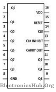
- Input Pin:
- Reset Pin (Pin 15) – The counter is reset to the zero position by this pin. Suppose you wish that the counter will only count till third position then you need linked the fourth pin with 15 pin. So after reaching to the third output it will automatically begin its counting from zero.
- Clock Pin (Pin14) – In each of the timing pin 14 moves at high the output will be given to you. From the initial clock pulse output will be received at the pin 3 likewise for the next clock pulse output will be received at the pin 2 and so on.
- Clock Inhibit Pin (Pin 13) – The counter is switched to “on” and “off” by this pin. If you need that the counter to be switched off then for that pin 13 must be at high state. If the pin is at high then it will disregard the clock pulse without paying attention that how much time you press the switch i.e. the count will not go forward. Pin 13 in our circuit is grounded.
- Output Pin (Pin Q0- Q9) -It is used to get the input in chronological order. Like pin 3 will give you the output for the first pulse and so on.
- Ground Pin (Pin 8) and Supply pin (pin 16) – For the proper working of these IC these pins are used to give ground as well as power supply.
- Carry out Pin (Pin 12) – These pins are used to link one or more CD4017 IC with each other. Suppose you have a desire to connect one more CD4017 IC then attach pin 12 to the clock input to its next one. The carry pin of first CD4017 is connected to clock input of the second and the carry pin of the second is connected to the clock input of the third and so on. In our circuit we left this pin as we have desire of only one IC in our circuit.
How Clap Switch Circuit Works?
At the time when some one slap in front of the Mic the sound signal is converted into the electrical signal by the condenser microphone.These signals are then given to the transistor T1 base which in return trigger the IC1 pin2. And with the help of the formula shown below the time period for which the output stay in the high position can be calculated –
T = 1.1*R5*C4
At the moment the output from the IC1 pin 3 is given to CD4017 decade counter 14 pin, which supply a clock pulse for the proper working of IC2. The counting of the CD4017 begins from the zero after getting the clock input. And it moves to forward one by one at each time whenever pin 14 moves to high (as in front of the mic we clap). Like we get output from the pin 2 for the first clap i.e. Q1 and LED1 will shine and the device connected to relay start operating . While for the second clap output will receive at pin 4 and LED2 will shine while at this time LED1 turn off and so on. At each output point you need to attach the individual relay .10 individual devices can be controlled with the help of this circuit just connect the relay at appropriate outputs of CD4017.
Note: For some more interesting projects and circuit diagrams, visit Mini Projects on Electronics.

20 Responses
Hi, i have completed many projects on avr microcontroller like automatic controlled home appliances, controlling motor speed using pwm , line follower robot,etc. Now i want to work on a practical project like the delhi metro system, etc using avr microcontroller only. Can you please suggest me a big project along with its technical details.I’ll really appreciate your help.
thnks a lot, it’s very useful but there is a small mistake on the diagram. cd4017 has vcc on pin 16 rather thn pin 1.
and I wish if u provide pcb layout of the circuit thn it’s better. and one more thing, kindly name the relay name using here
hi…
Can you please suggest a circuit that will allow each appliances on by clapping sequentially without turning the previous one off when I clap next time and will all of them be off when I clap the last ?
How many Appliances you want to switch on??If you want more number you should use a microcontroller..
if u have video on this circuit diagram then plz share with us m totally confused…………..
Can this work on an electric fan? Every clap increases the level of the fan? Where should I connect the circuit then?
Hi, Yes. You can probably use it increase the speed level of fan but the circuit might become complex. We haven’t tested it but you can use regulator with different settings at each relay.
if u have a video plz share it ……………………
How many volts of Relay use in this circuit. and the IC CD4017 thats have 16 pin and in this diagram 9 pins are used and others are where?
Hi, The relay used here is a 5V relay. CD4017 is a 16 pin DiP. The pins mentioned in the circuit are used and others can be ignored for this project.
hie can l have the components layout
Does the 8 pin of 555 goes to 14 of 4017
Hi,
Sorry. That is Pin 3. It goes to Pin 14 of 4017.
No as CD 4017 RECEIVES THE OUTPUT FROM THE 555 TIMER IC AND THE OUTPUT OF 555 TIMER IS COMING FROM THE PIN3 AS IT IS MENTION IN THE DATASHEET
do this circuit work? can I make this on PCB?
Is this a analog to digital converter … i mean can i use this circuit as a analog to digital converter .. ?
Where can I put the load? can I use a light bulb for the load? and the system will act as a dimmer.
Pls state the polarity of the cap’s
is this really working
Is we use ir for wireless control