In this tutorial, let us try to understand the need for a logic level converter, different ways to shift logic levels and finally how a Bidirectional Logic Level Converter works. This is very important if you want to connect 5V devices like Arduino to 3.3V devices like ESP8266 or Nokia 5110 LCD.
Outline
ToggleWhat is Logic Level?
Logic Level of a signal is the voltage or state in which it can exist. In the World of Digital Electronics, the inputs and outputs are allowed to have only two voltage levels or states, which is usually referred to a Logic 1 and Logic 0, or ON and OFF or TRUE and FALSE or HIGH and LOW.
Depending on the type of the Logic Family, the voltages for these logic levels vary. If we take a trip down the memory lane, then we can remember some of the logic families as:
- RTL (Resistor – Transistor Logic)
- ECL (Emitter – Coupled Logic)
- DTL (Diode – Transistor Logic)
- TTL (Transistor – Transistor Logic)
- PMOS (P-type MOS Logic)
- NMOS (N-type MOS Logic)
- CMOS (Complementary MOS Logic)
Each logic family is defined with its own logic voltage levels corresponding to logic High and Logic Low and their thresholds for both input and output. Let us focus of the two of the important logic families in the history of semiconductors: the TTL and the CMOS.
The following images shows input and output voltage thresholds for 5V TTL, 5V CMOS and 3.3V TTL Logic Families.
In the above image there are some symbols like VIL, VIH, VOL, etc. The following table gives you the meaning of those symbols.
|
VIL |
Input Voltage Low | Maximum voltage from Ground which is considered as Logic LOW input. |
| VIH | Input Voltage High |
Minimum voltage from VCC which is considered as Logic HIGH input. |
|
VOL |
Output Voltage Low | Maximum voltage from Ground which is considered as Logic LOW output. |
| VOH | Output Voltage High |
Minimum voltage from VCC which is considered as Logic HIGH output. |
Why Do We Need to Shift Logic Levels?
For the sake of comparison, let us select the 5V TTL, 5V CMOS and 3.3V CMOS Logic Families (as CMOS became the dominating technology in modern VLSI and TTL is popular in earlier “74” series of ICs).
What if we want to connect a 5V device with a 3.3V device or vice-versa? If you look closely at the above image with threshold voltages, then you can understand the problem.
For example, if you want to connect a 3.3V CMOS device with a 5V TTL device, then there should not be any problem as logic HIGH output of 3.3V CMOS device is between 2.4V and 3.3V and logic HIGH input of 5V TTL device is between 2V and 5V.
But what if you want to connect the other way i.e., a 5V TTL device with a 3.3V CMOS device? Then we have a problem. The logic HIGH input of 3.3V CMOS device is between 2V and 3.3V whereas the logic HIGH output of 5V TTL device is between 2.4V and 5V, which is significantly more than what the 3.3V device can handle.
Most 3.3V device can tolerate up to 3.6V and anything more than that will fry the IC. So, you have to take extreme care while connecting ICs or devices with different logic levels.
There are two ways in which you can solve this problem. One is the crude way of using a Voltage Divider circuit and the other way (also a better way) is to use Logic Level Converter or Logic Level Shifter.
Simple Voltage Divider
Since there is no problem in connecting a 3.3V device with a 5V device, you can use a voltage divider circuit when you want to connect a 5V device with a 3.3V device.
I made a dedicated tutorial on basics of voltage divider. So, for more in-depth information, take a look at the “VOLTAGE DIVIDER CIRCUIT” tutorial.
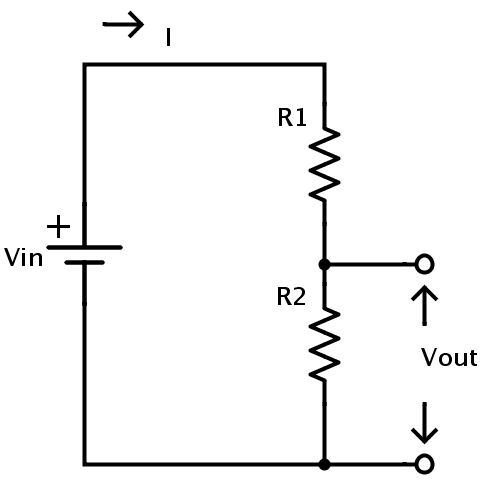
A voltage divider circuit simply converts a high input voltage (say 5V) to a low output voltage (like 3.3V) by using only two resistors.
From basic circuit theory, we can deduce the equation for VOUT as:
VOUT = (VIN * R2) / (R1 + R2)
In the above circuit, let us assume that VIN is 5V and VOUT is 3.3V. If we chose R1 as 1 kΩ, then using the above equation we get R2 as 1,914 Ω. The resistor with closest value to this result is 2.2 kΩ.
If we use the above equation with VIN as 5V, R1 as 1 kΩ and R2 as 2.2 kΩ, then we get VOUT as 3.4V, which is an acceptable value for 3.3V logic devices.
However, voltage divider is not an ideal solution for logic level conversion. Use this method only for slow signals and for switch inputs. It is not a reliable method for use in high-speed signals like I2C or SPI.
Bidirectional Logic Level Converter
Over the years, we have seen a lot of 3.3V devices like Raspberry Pi, ESP8266, ESP32, Nokia 5110 LCD, HC-05 Bluetooth Module, BMP180 Barometric Pressure Sensor etc.
If you want to connect a 3.3V I2C or SPI Sensor to a 5V device like Arduino with support for two-way communication, then the solution is to use an External Level Shifter or a Logic Level Converter.
The Logic Level Converter presented here supports bidirectional level shifting by using one MOSFET per bus line and it also protects the low voltage side from spikes at the high voltage side.
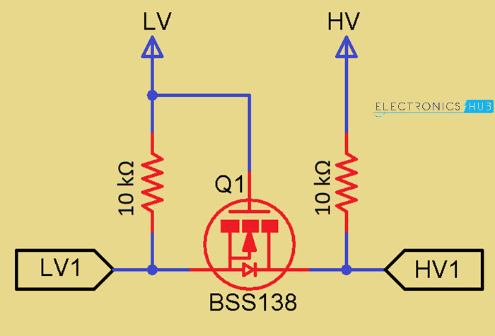
Consider the following circuit consisting of an N-Channel MOSFET with internal Drain – Substrate Diode (it is important to have one). Let us divide the circuit into two parts the left side or the low voltage side and the right side or the high voltage side.

Each side has different supply voltages and also different logic levels. The bus in the low voltage side is pulled HIGH to 3.3V and also the device power supply on this side is 3.3V.
The right-side bus is pulled HIGH to 5V and the device power supply voltage is 5V. The Gate of the MOSFET must be connected to low voltage power supply i.e., 3.3V in this case. The Source and Drain of the MOSFET are connected to low voltage bus and high voltage bus respectively.
This simple circuit acts a bidirectional logic level shifter.
How Bidirectional Logic Level Converter Works?
Let us now see how the above setup works as a bidirectional logic level converter. To understand the working clearly, let me divide the operation into three states.
Standby State
In the first state neither devices i.e., device on low voltage side or device on high voltage side is pulling the bus low. In this case, the low voltage bus is pulled high to low voltage
As both the Gate and Source of the MOSFET are connected to 3.3V, VGS is 0V, which is below the threshold voltage of the MOSFET. As a result, the MOSFET is not conducting and this allows the high voltage bus to be pulled high to 5V.
So, in this state, both sides of the bus are at logic HIGH but at different voltage levels.
3.3V Device Pulls Down the Bus
The second state is when the 3.3V device pull the bus down to logic LOW level. The gate of the MOSFET is still at 3.3V but the source becomes low. As a result, the VGS becomes 3.3V, which is greater than the threshold voltage of the MOSFET and this allows the MOSFET to conduct.
Since the MOSFET is now conducting, the high voltage bus is pulled down by the 3.3V device to logic LOW. Hence, both sides of the bus are at logic LOW of same voltage level.
5V Device Pulls Down the Bus
In the third state, the 5V device pulls the high voltage side bus to logic LOW level. Through the Drain – Substrate diode, the low voltage side is pulled down until the VGS reaches the threshold voltage.
The MOSFET now starts conducting which will further pull the low voltage side bus to logic LOW voltage level by the 5V device. Even in this case, both sides of the bus are at logic LOW level at same voltage.
So, if you combine the three states, we can conclude that logic levels are shifted in both the direction.
Phillips published a beautiful Application Note on this topic called “Bi-directional level shifter for I²C-bus and other systems”. Search for “AN97055” for more information.
Logic Level Converter Modules
Many module manufacturers are combining 4 such MOSFET based level shifting circuits to develop a 4- bus or 4-channel Logic Level Converter Modules.
The schematic of one such module is shown in the following image.

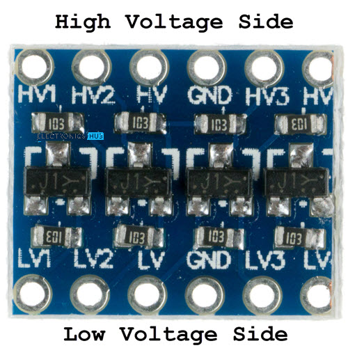
If you take a look at the image of a typical 4-channel Level Shifter Module, it consists of 12 pins in two rows. The top row consists of high voltage supply and ground pins (HV and GND) and 4 high voltage channels (HV1, HV2, HV3 and HV4).

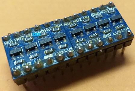
The bottom row consists of low voltage supply and ground (LV and GND) and 4 low voltage channels (LV1, LV2, LV3 and LV4). I combined two such modules to make an 8-channel Logic Level Converter.
Conclusion
In this tutorial, you learned about Logic Levels, need for logic level conversion, simple voltage divider based voltage level conversion and a very useful Bidirectional Logic Level Converter with schematic and module.


3 Responses
Hello,
Making a bunch of logic level conversion boards for my work’s prototyping lab; I know I could just buy a bunch from a prototyping group like sparkfun or adafruit, but I’d like to make my own to better understand it and be able to place logic level converter circuits on my final board designs in the future.
My main question; you don’t necessarily need a ground pin on these little prototyping boards, do you? The circuit in theory only needs the LV and HV connections, and the ground is only involved when one side of the bus is pulled down. if you have a ground rail (on a breadboard, per se) connected to all 3.3V and 5V elements in the circuit, then you don’t need a ground connection on the converter?
TL;DR: The logic level prototyping board in the example above have ground pins, but those ground pins aren’t actually connected to anything in the logic level converter circuit, correct?
Both the LV and HV grounds should be common (either on the logic level conversion board or at the power supply). GND is common reference for both HV and LV.
Yeah.
My guess is that the gnd is a pass through trace on the board and not serving any useful purpose.
—
By contrast on the little nunchuck i2c level shifter breakout boards they have a softer just like this but also there is a justification for gnd as they also contain a 5 to 3.3v regulator to power the nunchuck.