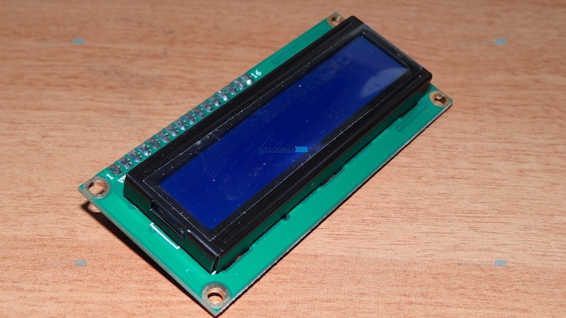
The next important project after Blinking LEDs with any microcontroller is to display characters on a LCD. In this project, we will see how to interface a LCD with LPC2148 Microcontroller and when we say LCD, a 16 X 2 Alphanumeric LCD module to be specific.
Before going to the actual project, we will discuss a few things about 16 x 2 LCD display. A LCD display or liquid crystal display is a display module with liquid crystals and backlight by LEDs. A 16 x 2 LCD display consists of two rows of display with each row consisting of 16 characters.
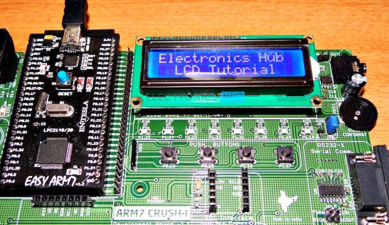
Interfacing 16 X 2 LCD with LPC2148 ARM 7 Microcontroller
The most common type of 16 x 2 LCD display available in the market is JHD162A with either HD44780 or KS0066U Display Controller. HD44780 is manufactured by Hitachi and KS0066U is manufactured by Samsung. Both the controllers are compatible with each other.
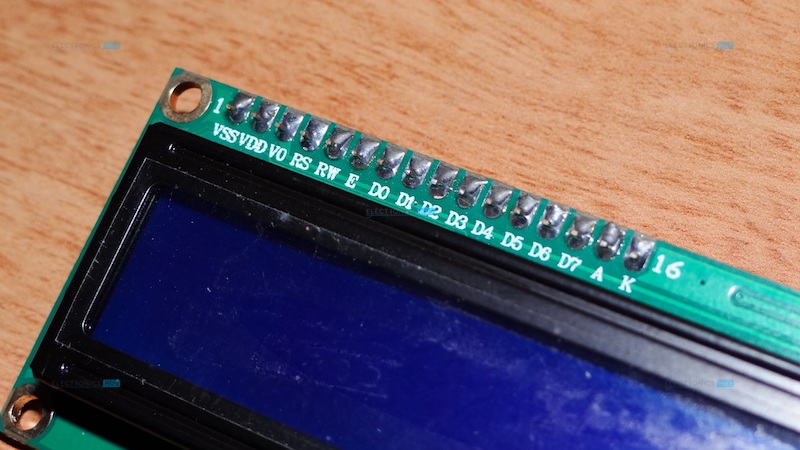
This LCD Module has 16 pins and operates on 5V supply. The standard pin out of a 16 x 2 LCD display is as follows.
Pin Configuration
| Pin Number | Name | Function |
| 1 | VSS | Power supply (GND) |
| 2 | VDD | Power supply +5V |
| 3 | VO or VEE | Contrast adjustment: through a variable resistor. |
| 4 | RS | Selects command register when low; and data register when high |
| 5 | R/W̅̅ | Low to write to the register; High to read from the register |
| 6 | E | Sends data to data pins when a high lo low pulse is given |
| 7 | DB0 | Data bus line |
| 8 | DB1 | Data bus line |
| 9 | DB2 | Data bus line |
| 10 | DB3 | Data bus line |
| 11 | DB4 | Data bus line |
| 12 | DB5 | Data bus line |
| 13 | DB6 | Data bus line |
| 14 | DB7 | Data bus line |
| 15 | A | Power supply for LED Backlight (+5V) |
| 16 | K | Power supply for LED Backlight (GND) |
From the pin configuration, it is clear that the pins can be sorted according to Power pins, control pins and data pins. Power pins i.e. pins 1, 2, 3, 15 and 16 are used to supply for the module as well as the backlight LEDs. The voltage to the Contract Adjust Pin (Pin 3 or VEE) is usually given from a Potentiometer and will control the contrast of the actual display when the POT is adjusted.
There are 8 data pins for transmitting 8 – bits of data i.e. 1 byte of data at a time. The LCD can be used in either 8 – bit mode or 4 – bit mode. In 4 – bit mode, only 4 of the 8 data lines will be utilized for transmitting the data.
The remaining three pins i.e. RS (Pin 4), RW (Pin 5) and E (Pin 6) are called the Control Pins and are very important pins.
The RS pin, which is short for Register Select pin, is used to select either Instruction Register when it is LOW or Data Register when it is HIGH.
The RW pin or the Read / Write Pin is used for selecting Read Mode or Write Mode. When RW is HIGH, read mode is selected and data is read from the register. When RW is LOW, write mode is selected and data can be written in to the register.
Since we are using the write mode only, we can connect the RW pin to ground (through a pull down resistor).
The Enable (E) pin, as the name indicates, is used to enable the execution of the data or instructions. The data or instruction are executed by the LCD module only when a HIGH to LOW pulse is given to the Enable pin i.e. only on the falling edge of a pulse.
Interfacing LCD Module with LPC2148
The circuit for interfacing a 16 x 2 LCD Module with LPC2148 MCU is shown in the following image.
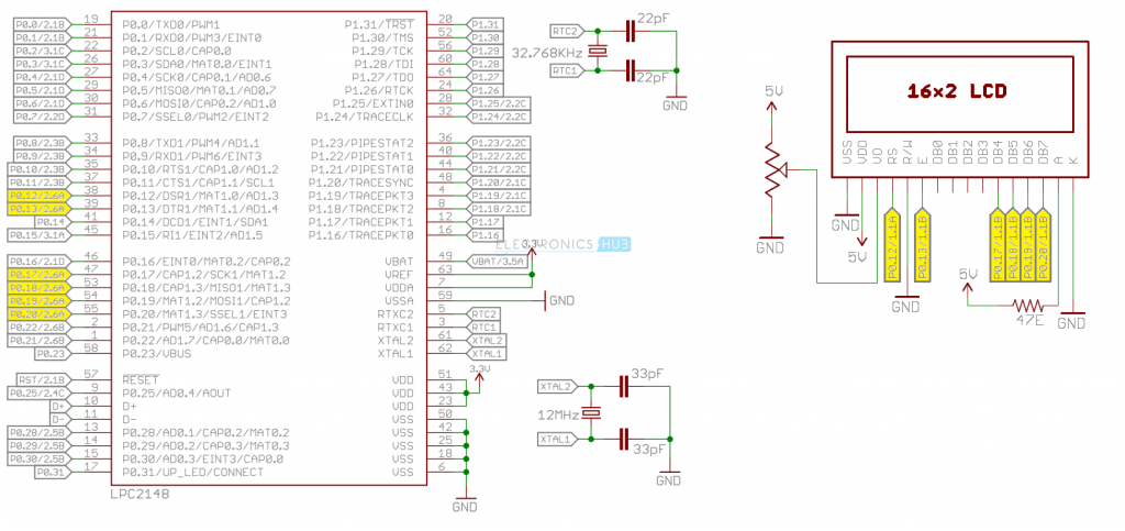
From the circuit diagram, the four data pins of the LCD (D4 – D7) are connected to P0.17 to P0.20 pins of the LPC2148. The control pins RS and E are connected to P0.12 and P.13 pins of the LPC2148 MCU.
It is clear from the circuit diagram that the LCD is used in 4 – bit mode. The advantage of using 4 – bit mode in LCD is it requires only 4 pins from the microcontroller, which is very important in resource intensive applications.
There is also a tradeoff of using the 4 – bit mode in LCD. Since only 4 – pins are used, we can send only 4 – bits of data at a time. Hence, in order to send a byte of data, the time will be taken will double that of an 8 – bit mode.
If the number of I/O pins on a MCU are limited and timing is not an issue, then we can go for 4 – bit mode. Also, the 4 – bit mode requires additional lines of code for shifting the data in the lower nibble to higher nibble every time we send an instruction or data.
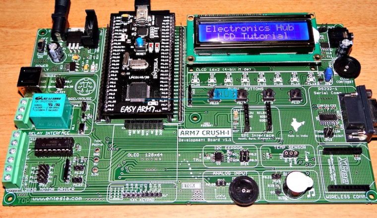
Important Note: The ARM7 MCUs and in particular the LPC2148 MCU works on a 3.3V supply. The ARM7 development board used in the project has a separate 5V supply for the LCD module and doesn’t draw any power from the MCU.
While interfacing the 5V LCD module with a 3.3V MCU like a LPC2148, there is a chance that the connection might work if connected directly. In this case, we need to use a Level Shifter IC as an intermediate module between the MCU i.e. LPC2148 and the LCD Module.
The commonly used level shifter is HEF4050B, which is a Hex non – inverting buffer. It can be used to convert logic levels to standard TTL levels. There are other buffers or Level Shifters in 74 series if ICs.
Initializing the LCD Module
After connecting the LCD module as per the circuit diagram, the first step is to initialize the LCD module. For that, we need to use some of the commands for the LCD in our program. The following table shows a list of commands used for configuring the LCD Module and also their respective functions.

The above table seems confusing and is difficult to understand. Hence, the following table will give you a simplified list of LCD commands and their respective functions.
| 1 | Function Set: 8 – bit Mode, 1 Line, 5×7 Dots | 0x30 |
| 2 | Function Set: 8 – bit Mode, 2 Line, 5×7 Dots | 0x38 |
| 3 | Function Set: 4 – bit Mode, 1 Line, 5×7 Dots | 0x20 |
| 4 | Function Set: 4 – bit Mode, 2 Line, 5×7 Dots | 0x28 |
| 5 | Entry Mode | 0x06 |
| 6 | Display off Cursor off | 0x08 |
| 7 | Display on Cursor on | 0x0E |
| 8 | Display on Cursor off | 0x0C |
| 9 | Display on Cursor blinking | 0x0F |
| 10 | Shift entire display left | 0x18 |
| 11 | Shift entire display right | 0x1C |
| 12 | Move cursor left by one character | 0x10 |
| 13 | Move cursor right by one character | 0x14 |
| 14 | Clear Display (also clear DDRAM content) | 0x01 |
| 15 | Set DDRAM address or cursor position on display | 0x80 + address |
| 16 | Set CGRAM address or set pointer to CGRAM location | 0x40 + address |
Out of these commands, we are going to five commands in our project. They are listed below along with their function in the project.
- 0x28: This command is used to enable 4 – bit mode for a 2 line module with 5 x 7 dots per character.
- 0x0C: It is a display switch command and is used to turn on the display and turn off the cursor.
- 0x01: This command is used to clear the contents of the display. To be more specific, it clears the contents of the DDRAM.
- 0x80: It is used to set the cursor position to the beginning of the first line. It also means that the DDRAM address is set with this value.
- 0xC0: It is also used to set the position of the cursor but this time, the position is set to the starting position in the second line.
Program for Interfacing LCD with LPC2148
As we have seen in the previous tutorial how to setup the PLL so that the CPU clock is running at 60 MHz (maximum for LPC2148), we will include that in this code as well. The steps for writing the programming the LCD interface with LPC2148 will be as follows.
- Setup the PLL Module
- Initialize the LCD Module
- Send the data to the LCD Module
More detailed steps are explained with the program.
#include<lpc214x.h>
/* Define 17, 18, 18 and 20 pins of PORT0 as the data pins and 12 and 13 pins of PORT0 as RS and E pins for the LCD*/
#define LCD 0x001e0000
#define RS (1<<12)
#define E (1<<13)
/* Define the functions used in the program*/
void delay (int);
void cmd (unsigned char);
void display (unsigned char);
void LCDinit (void);
void string (char *);
/* Function definition of delay function */
void delay (int d)
{
unsigned int i=0;
for(;d>0;d–)
{
for(i=11998;i>0;i–);
}
}
/* Function definition of cmd function. It is used to send initializing commands to the LCD module. Hence, the RS pin is set to LOW. Also the code is written two times: once the 4 bits are received, they are shifted and the next 4 bits are captured*/
void cmd (unsigned char c)
{
IOPIN0 = (IOPIN0 & 0xffe1ffff) | ((c&0x000000f0)<<13);
IOCLR0 = RS;
IOSET0 = E;
delay(10);
IOCLR0 = E;
IOPIN0 = (IOPIN0 & 0xffe1ffff) | ((c&0x0000000f)<<17);
IOCLR0 = RS;
IOSET0 = E;
delay(10);
IOCLR0 = E;
}
/* Function definition of display function. It is used to send the actual data to the LCD module. Hence, the RS pin is set to HIGH*/
void display (unsigned char c)
{
IOPIN0 = (IOPIN0 & 0xffe1ffff) | ((c&0xf0)<<13);
IOSET0 |=RS;
IOSET0 |=E;
delay(10);
IOCLR0 |=E;
IOPIN0 = (IOPIN0 & 0xffe1ffff) | ((c&0xf)<<17);
IOSET0 |=RS;
IOSET0 |=E;
delay(10);
IOCLR0 |=E;
}
/*Function to capture the data and pass it to the display command */
void string (char *p)
{
while(*p)
{
display(*p++);
}
}
/* Function definition of the LCD initializing function. The commands to initialize the LCD Module are given using this function */
void init (void)
{
cmd(0x00000028);
cmd(0x0000000c);
cmd(0x00000001);
cmd(0x00000080);
}
int main()
{
PINSEL0=0x00;
PINSEL1=0x00;
IODIR0=LCD|RS|E;
/* Initialize the PLL and assigning it as the system clock and peripheral clock */
PLL0CON = 0x01;
PLL0CFG = 0x24;
PLL0FEED = 0xaa;
PLL0FEED = 0x55;
while(!(PLL0STAT & 0x00000400));
PLL0CON = 0x03;
PLL0FEED = 0xaa;
PLL0FEED = 0x55;
VPBDIV = 0x01;
LCDinit();
while(1)
{
string(“Electronics Hub”);
cmd(0xc0);
string(” LCD Tutorial “);
while(1);
}
}

2 Responses
In command and data subroutine, why are you shifting it by 13 bit?
IOPIN = 11111111111xxxx11111111111111111
xxxx is command code
For example 0x28 command, xxxx actually change to 1010, not 10100