The IC 555 is one of the most popular and most widely used IC’s. It is a versatile and extremely robust integrated circuit that is used in many applications like timers, wave generators (pulse) and oscillators.
The IC555, popularly known as the 555 Timer, was developed by Hans Camenzind of Signetic Corporation in the year 1971.
It was released in two parts: NE 555 and SE 555. The NE 555 parts were of commercial usage with a temperature range of 00C to 700C and the SE 555 parts are designed to meet the military standards with a temperature range of -550C to 1250C. It is a monolithic IC and was the first commercially available timer IC’s.
Understanding 555 Timer Features
Some of the important features of the 555 timer are
- The 555 timer can be operated at a wide range of power supplies ranging from 5 V to 18 V.
- It is available in 3 different packages: 8-pin Metal Can package, 8-pin DIP and 14-pin DIP.
- Timing can be anywhere from microseconds to hours.
- It can operate in both astable and monostable modes.
- High output current.
- It has an adjustable duty cycle.
- It is TTL compatible due to its high output current.
- The output can source or sink a current of 200mA to the load.
- It has a temperature stability of 0.005% per 0C.
Know more from 555 Timer datasheet
Different Modes Of Operation in 555 Timer
Generally, the 555 timer can be operated in three modes: Astable, Monostable (or one-shot) and Bistable.
Astable Mode
In this mode, the 555 work as a free running mode. The output of astable multivibrator will continuously toggle between low and high, there by generating a train of pulse, which is why it is known as pulse generator.
It is a best example for a perfect square wave generator. They are used as an inverter and also used in many of the internal part of the radio. Selecting a Thermistor as a timing resistor allows the use of the 555 in a temperature sensor.
Read : Astable Mode
Monostable Mode
In the monostable mode, as the name suggests, it stays in its stable state until and unless an external trigger is applied. In this mode, the 555 functions as a “one-shot” pulse generator. The best application of a monostable is to introduce a time delay in to a system.
Applications comprise many things viz., timers, missing pulse detection also included bounce free switches, touch switches as well as frequency divider, capacitance measurement and pulse-width modulation (PWM) and many more.
Read : Monostable Mode
Bistable Mode
In the bistable mode, the IC 555 acts as a flip-flop as it has two stable states. It can be used to store 1-bit of data. It is not a great choice for implementing a flip-flop.
Read:Bistable Mode
Pin Configuration of 555 Timer
The 555 Timer is available in 8-pin Metal Can Package, 8-pin Mini Dual in-line Package (DIP) and 14-pin DIP. The 14-pin DIP is IC 556 which consists of two 555 timers.
The 8-pin DIP is most commonly used. The pin out diagrams of 555 Timer in both the 8-pin packages is shown below.
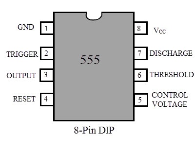
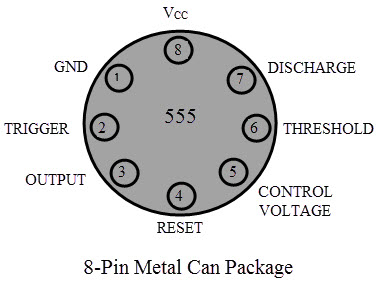
The names and numbers of all the pins along with their descriptions are tabulated below.
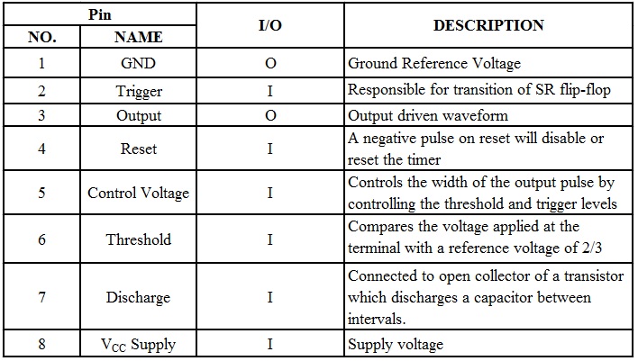
Pin 1 – Ground (GND)
Ground reference voltage (low level 0V). All the voltages are measured with respect to this terminal.
Pin 2 – Trigger Terminal
It is responsible for SET and RESET transitions of the flip-flop. The amplitude of the external trigger pulse will influence the output of the timer. The output goes high and the timing interval starts when the input at trigger pin falls below half of Control voltage (i.e. 1/3 of the VCC).
Pin 3 – Output Terminal
Output driven waveform is available at this pin. It is driven to 1.7 V below VCC. Two types of loads can be connected to the output. One is Normally OFF load, which is connected between Pins 3 and 1 (GND) and the other is Normally ON load, which is connected between pins 3 and 8 (VCC).
Pin 4 – Reset Terminal
A negative pulse on this pin will disable or reset the timer. The timer will begin only when the voltage on this pin is above 0.7 V and hence it is normally connected to VCC when not used.
Pin 5 – Control Voltage
It controls the threshold and trigger levels and hence the timing of the 555. The width of the output pulse is determined by the control voltage. The output voltage can be modulated by an external voltage applied to this pin. Generally, it is connected to ground through a 10µF capacitor when not in use in order to eliminate any noise.
Pin 6 – Threshold Terminal
The voltage applied at this terminal is compared with a reference voltage of 2/3 VCC. When the voltage at this terminal is greater than 2/3 VCC, the flip-flop is RESET and the output falls from High to Low.
Pin 7 – Discharge
It is connected to the open collector of the internal NPN transistor which discharges the timing capacitor. When the voltage at this pin reaches 2/3 VCC, the output toggles from high to low.
Pin 8 – VCC or Supply
A supply voltage in the range of 5V to 18V is applied to this terminal.
555 Timer Internal Circuit Diagram
The internal block diagram of a 555 timer is shown below. It consists of the following
- Two Comparators
- An SR flip-flop
- Two transistors
- A resistive network
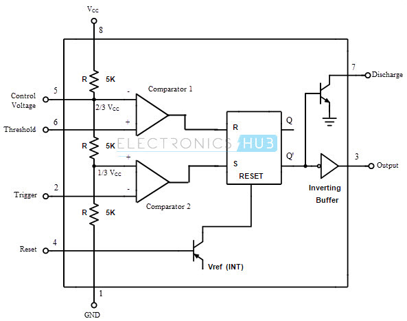
The comparators are the basic Op-amps. The comparator 1, which provides the R input, compares the threshold voltage with a 2/3 VCC reference voltage.
The comparator 2, which provides the S input to the flip-flop, compares the trigger voltage with a 1/3 VCC reference voltage.
The resistive network of three resistors will act as a voltage divider circuit. The values of these resistors are 5KΩ each. These three 5K resistors are responsible for the name “IC 555”.
Out of the two transistors, one transistor is a discharge transistor. The open collector of this transistor is connected to the discharge pin (Pin 7) of the IC. According to the output of the flip-flop, this transistor either goes into saturation or cut-off.
When the transistor is saturated, it provides a discharge path to the capacitor that is connected externally. The base of the other transistor is connected to the reset terminal (Pin 4) which resets the timer irrespective of the other inputs.
555 Timer Working
The three 5KΩ resistors form a voltage divider network. This network provides two reference voltages to two comparators 2/3 VCC to the inverting terminal of the upper comparator (comparator 1) and 1/3 VCC to the non-inverting terminal of the lower comparator (comparator 2).
The inverting terminal of the upper comparator is connected to the control input. Generally, control input is not used and is connected to 2/3 VCC. The other input of the upper comparator is threshold and its output is connected to the R input of the flip-flop.
When the threshold voltage is greater than 2/3 VCC (i.e. the control voltage), then the flip-flop is RESET and the output goes LOW. This will turn the discharge transistor ON (transistor goes to saturation) and provides a discharge path to any externally connected capacitor.
A trigger input is connected to the inverting terminal of the lower comparator. When the trigger input is less than the reference voltage (1/3 VCC), the lower comparator’s output is high.
This is connected to the S input of the flip-flop and hence the flip-flop is SET and the output goes HIGH and the timing interval starts. As the output is high, the discharge transistor is turned OFF and allows charging of any capacitor connected to it externally.
Hence, in order for the output to go HIGH, the trigger input should be less than the reference voltage momentarily. The output is low when the threshold voltage is greater than 2/3 VCC, which resets the flip-flop and hence the output.
Introduction to Time Constant RC
Meeting timing requirements is a high priority task in most of the operations. For example, the heating process of a metal or a material in an industry is time limited.
Hence meeting the specific time requirements can be achieved by timer circuits.
A basic timer circuit is shown below. It consists of a charging circuit, a comparator and an output unit.
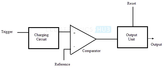
The charging circuit consists of a resistor and a capacitor. When a series combination of an RC circuit is applied with a DC voltage, the time taken for the capacitor to charge to the peak value is controlled by the resistor.
The charging time is proportional to the value of the resistance. The rate at which the capacitor charges in an RC circuit is given by Time constant.
RC Time Constant, generally called Tau (represented by the symbol τ), is the time constant of an RC circuit which is the time taken by the Capacitor to charge through the Resistor by approximately 63.2 % of the difference between initial and the final values.
It is also equal to the time taken by the capacitor to discharge to 36.8%. Time constant of an RC circuit is equal to the product of R and C.
τ = RC
As mentioned earlier, when the trigger input falls below 1/3 VCC, the output of the timer goes high and the period for which this stays high is determined by the RC time constant.
The pulse width and the frequency of the output of the 555 timer are determined by the RC time constant.
Choosing Timing Components for RC circuit in Timer
A 555 timer can provide delays from microsecond to hours depending on the values of R and C in the charging circuit. Hence it is very important to choose appropriate values for resistors and capacitors.
When the 555 timer is operating in Astable mode, then it requires an RC circuit consisting of two resistors and a capacitor. And in case of monostable mode of operation, the RC circuit comprises of a resistor and a capacitor.
Timing Capacitor
Choosing capacitors with large capacitances will be a problem. This is because electrolyte capacitors with large capacitances often tend to have wider tolerance limits. So the actual values and the marked values may have a significant difference.
Large capacitance electrolyte capacitors will have high leakage currents which can affect the timing accuracy as the capacitor charges. When choosing capacitors with large capacitance and low leakage current, Tantalum capacitors are a better option.
It is better to avoid electrolyte capacitors that have a high working voltage rating as they do not work efficiently when operated at a voltage 10% less than their rated voltage.
Hence, capacitors with working voltage greater than the VCC of the 555 timer should be chosen.
Timing capacitors with capacitance less than 100pF in order to produce short output pulses may also cause problems.
For capacitors with such low values, stray capacitance around the circuit might affect the capacitance of the timing capacitor.
Timing Resistor
When operating the 555 timer as an Astable multivibrator , the value of the timing resistor should be at least 1 Kilo Ohms. If the idea is to build a low power consumption circuit, then it is better to have higher values for the timing resistors.
But there is a disadvantage in choosing resistors with higher resistances as they lead to inaccuracies in timing. In order to minimize these inaccuracies, the value of the timing resistor shouldn’t be more than 1 Mega Ohms.
Trigger Pulses
The Pin 2 in the 555 timer is a trigger input. When the trigger input goes below the reference voltage i.e. 1/3 VCC, the output of the timer is high and the timing interval begins.
The trigger pulse should momentarily go below the reference voltage and the duration is important as it should not be longer than the output pulse.
Trigger pulses are generally identified by a narrow negative going spike. A differentiator circuit made from a capacitor and a resistor will produce two symmetrical spikes but a diode is used to eliminate the positive going spike.
The duration of the pulse is determined by the differentiator circuit (i.e. it depends on the capacitor and resistor).
Applications
Since the introduction of the IC 555 in the early 70’s, it has been employed in numerous circuits and applications by researchers as well as hobbyists. Some of the important areas of applications of the 555 timer are:
- Pulse Generation
- Time Delay Generation
- Precision Timing
- Sequential Timing
- Pulse Width Modulation (PWM)
The typical applications of a 555 timer can be differentiated by the mode of operation. Depending on the mode in which it is operated i.e. either in astable or in monostable mode, some of the applications of IC 555 are:
- Frequency Divider
- Linear Ramp Generator
- Missing Pulse Detector
- Pulse Position Modulation
- Square Wave Generation
- Pulse Width Modulation
- Oscillator
- Tone Burst Generator
- Speed Warning Device
- Regulated DC – to – DC Converter
- Voltage – to – Frequency Converter
- Low Cost Line Receiver
- Cable Tester

6 Responses
how can a 555 timer be use to build an alarm system
Read the post: Water Level Alarm using 555 Timer to get an idea about how to build an alarm system using 555 timer.
this Block diagram of 555 timer is technically different in each description i have read anywhere in books ,in magazines,in websites posts. But it seems very easy to understand. Nice job done.
Very True , the content is very crisp.
how can a 555 timer be to build astable multivabrator
Thanks for good information